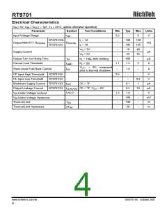
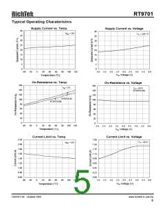
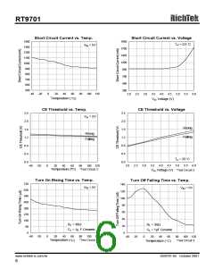
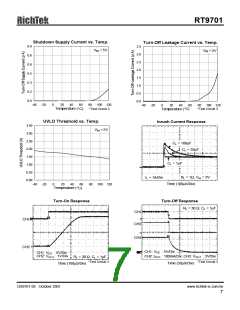
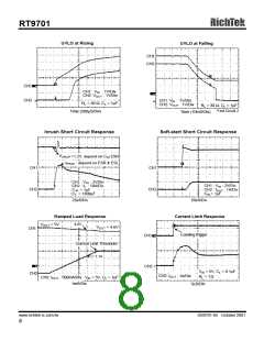
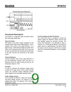
RT9701
Applications Information
Ferrite beads in series with all power and ground
lines are recommended to eliminate or significantly
reduce EMI. In selecting a ferrite bead, the DC
resistance of the wire used must be kept to a
minimum to reduce the voltage drop.
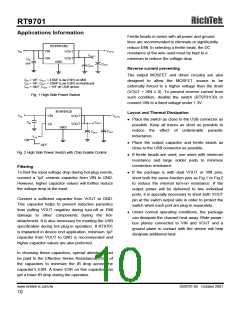
RT9701CBL
VIN
VIN
VOUT2
V
IN
VOUT
VOUT1
VOUT
CIN
1 F
GND
µ
COUT
COUT
Reverse current preventing
The output MOSFET and driver circuitry are also
designed to allow the MOSFET source to be
externally forced to a higher voltage than the drain
(VOUT > VIN ≥ 0). To prevent reverse current from
such condition, disable the switch (RT9701CB) or
connect VIN to a fixed voltage under 1.3V.
µ
µ
CIN = 1 F, COUT = 470 F (Low ESR) on M/B
µ
µ
CIN = 1 F, COUT = 330 F (Low ESR) on Notebook
µ
µ
CIN = 10 F, COUT = 1 F on USB device
Fig. 1 High Side Power Switch
RT9701CB
Layout and Thermal Dissipation
VIN
V
IN
VOUT2
VOUT
z Place the switch as close to the USB connector as
possible. Keep all traces as short as possible to
reduce the effect of undesirable parasitic
inductance.
CIN
VOUT1
COUT
VOUT
CE
GND
COUT
VCE
ON
z Place the output capacitor and ferrite beads as
OFF
close to the USB connector as possible.
Fig. 2 High Side Power Switch with Chip Enable Control
z If ferrite beads are used, use wires with minimum
resistance and large solder pads to minimize
connection resistance.
Filtering
To limit the input voltage drop during hot-plug events,
connect a 1µF ceramic capacitor from VIN to GND.
However, higher capacitor values will further reduce
the voltage drop at the input.
z If the package is with dual VOUT or VIN pins,
short both the same function pins as Fig.1 or Fig.2
to reduce the internal turn-on resistance. If the
output power will be delivered to two individual
ports, it is specially necessary to short both VOUT
pin at the switch output side in order to protect the
switch when each port are plug-in separately.
Connect a sufficient capacitor from VOUT to GND.
This capacitor helps to prevent inductive parasitics
from pulling VOUT negative during turn-off or EMI
damage to other components during the hot-
detachment. It is also necessary for meeting the USB
specification during hot plug-in operation. If RT9701
is implanted in device end application, minimum 1µF
capacitor from VOUT to GND is recommended and
higher capacitor values are also preferred.
z Under normal operating conditions, the package
can dissipate the channel heat away. Wide power-
bus planes connected to VIN and VOUT and a
ground plane in contact with the device will help
dissipate additional heat.
In choosing these capacitors, special attention must
be paid to the Effective Series Resistance, ESR, of
the capacitors to minimize the IR drop across the
capacitor’s ESR. A lower ESR on this capacitor can
get a lower IR drop during the operation.
www.richtek-ic.com.tw
DS9701-05 October 2001
10

 RICHTEK [ RICHTEK TECHNOLOGY CORPORATION ]