RT9183
The maximum power dissipation depends on the thermal
resistance of IC package, PCB layout, the rate of
surroundings airflow and temperature difference between
junction to ambient. The maximum power dissipation can
be calculated by following formula:
Good board layout practices must be used or instability
can be induced because of ground loops and voltage drops.
The input and output capacitors MUST be directly
connected to the input, output, and ground pins of the
device using traces which have no other currents flowing
through them.
PD(MAX) = ( TJ(MAX) - TA ) /θJA
The best way to do this is to layout CIN and COUT near the
device with short traces to the VIN, VOUT, and ground pins.
Where TJ(MAX) is the maximum operation junction
temperature 125°C, TA is the ambient temperature and
the θJA is the junction to ambient thermal resistance.
The regulator ground pin should be connected to the
external circuit ground so that the regulator and its
capacitors have a“single point ground” .
For recommended operating conditions specification of
RT9183, where TJ(MAX) is the maximum junction
temperature of the die (125°C) and TA is the maximum
ambient temperature. The junction to ambient thermal
resistance (θJA is layout dependent) for SOT-223 package
is 115°C/W, SOT-223 package (F-Type) is 135°C/W,
SOP-8 package is 125°C/W, and TO-263 package is
45°C/W on standard JEDEC 51-3 thermal test board.
It should be noted that stability problems have been seen
in applications where “ vias ” to an internal ground plane
were used at the ground points of the device and the input
and output capacitors. This was caused by varying ground
potentials at these nodes resulting from current flowing
through the ground plane. Using a single point ground
technique for the regulator and it's capacitors fixed the
problem. Since high current flows through the traces going
into VIN and coming from VOUT, Kelvin connect the capacitor
leads to these pins so there is no voltage drop in series
with the input and output capacitors.
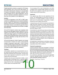
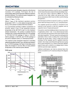
The maximum power dissipation depends on operating
ambient temperature for fixedTJ(MAX) and thermal resistance
θJA. For RT9183 packages, the Figure 4 of derating curves
allows the designer to see the effect of rising ambient
temperature on the maximum power allowed.
Optimum performance can only be achieved when the
device is mounted on a PC board according to the diagram
below:
PCB Layout
2400
TO-263
2000
GND
1600
1200
SOT-223
SOP-8
800
+
ADJ
V
EN
SOT-223
400
(F-Type)
0
OUT
0
25
50
75
100
125
Ambient temperature ((℃°C))
+
Figure 4
GND
V
IN
GND
SOP-8 Board Layout
DS9183-12 March 2007
www.richtek.com
11

 RICHTEK [ RICHTEK TECHNOLOGY CORPORATION ]