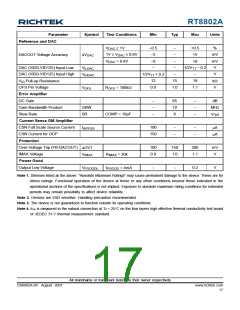
RT8802A
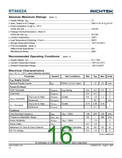
Parameter
Reference and DAC
Symbol
Test Conditions
Min
Typ
Max
Units
V
≥ 1V
−0.5
−5
−8
--
--
--
+0.5
+5
%
mV
mV
V
DAC
1V ≥ V
≥ 0.8V
DACOUT Voltage Accuracy
ΔV
DAC
DAC
V
DAC
< 0.8V
--
+8
DAC (VID0-VID125) Input Low
DAC (VID0-VID125) Input High
--
V
V
1/2V − 0.2
ILDAC
TT
--
--
V
1/2V + 0.2
IHDAC
TT
12
15
1.0
18
1.1
V
Pull-up Resistance
kΩ
V
ID
OFS Pin Voltage
0.9
V
OFS
R
= 100kΩ
OFS
Error Amplifier
DC Gain
--
--
--
65
10
8
--
--
--
dB
Gain-Bandwidth Product
Slew Rate
GBW
SR
MHz
V/μs
COMP = 10pF
Current Sense GM Amplifier
CSN Full Scale Source Current
CSN Current for OCP
Protection
100
150
--
--
--
--
I
μA
μA
ISPFSS
Over-Voltage Trip (FB-DACOUT)
IMAX Voltage
100
0.9
150
1.0
200
1.1
mV
V
ΔOVT
V
IMAX
R
= 20k
IMAX
Power Good
Output Low Voltage
--
--
0.2
V
V
I
= 4mA
PGOODL
PGOOD
Note 1. Stresses listed as the above "Absolute Maximum Ratings" may cause permanent damage to the device. These are for
stress ratings. Functional operation of the device at these or any other conditions beyond those indicated in the
operational sections of the specifications is not implied. Exposure to absolute maximum rating conditions for extended
periods may remain possibility to affect device reliability.
Note 2. Devices are ESD sensitive. Handling precaution recommended.
Note 3. The device is not guaranteed to function outside its operating conditions.
Note 4. θJA is measured in the natural convection at TA = 25°C on the four layers high effective thermal conductivity test board
of JEDEC 51-7 thermal measurement standard.
All brandname or trademark belong to their owner respectively
DS8802A-04 August 2007
www.richtek.com
17

 RICHTEK [ RICHTEK TECHNOLOGY CORPORATION ]