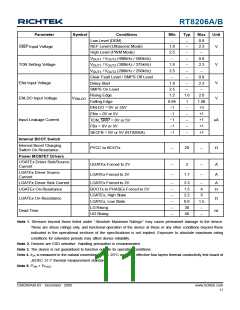
RT8206A/B
Parameter
Symbol
Conditions
Low Level (DEM)
Min
Typ
Max
Unit
--
--
--
--
0.8
2.3
--
REF Level (Ultrasonic Mode)
High Level (PWM Mode)
1.8
2.5
SKIP Input Voltage
V
V
/ V
/ V
/ V
(400kHz / 500kHz)
(300kHz / 375kHz)
(200kHz / 250kHz)
--
1.8
2.5
--
--
--
0.8
2.3
--
OUT1
OUT2
OUT2
OUT2
TON Setting Voltage
V
OUT1
V
V
OUT1
--
Clear Fault Level / SMPS Off Level
Delay Start
--
0.8
2.3
--
ENx Input Voltage
V
V
1.8
2.5
1.2
0.94
−1
--
SMPS On Level
Rising Edge
--
1.6
1
2.0
1.06
+3
ENLDO Input Voltage
V
ENLDO
Falling Edge
ENLDO = 0V or 25V
ENx = 0V or 5V
--
−1
--
+1
Input Leakage Current
−1
--
+1
μA
TON, SKIP = 0V or 5V
FBx = 0V or 5V
−1
--
+1
SECFB = 0V or 5V (RT8206A)
−1
--
+1
--
Internal BOOT Switch
Internal Boost Charging
Switch On-Resistance
PVCC to BOOTx
--
20
Ω
Power MOSFET Drivers
UGATEx Driver Sink/Source
Current
UGATEx Forced to 2V
LGATEx Forced to 2V
--
--
2
--
--
A
A
LGATEx Driver Source
Current
1.7
LGATEx Driver Sink Current
UGATEx On-Resistance
LGATEx Forced to 2V
BOOTx to PHASEx Forced to 5V
LGATEx, High State
LGATEx, Low State
LG Rising
--
--
--
--
--
--
3.3
1.5
2.2
0.6
30
--
4
A
Ω
5
LGATEx On-Resistance
Dead Time
Ω
1.5
--
ns
UG Rising
40
--
Note 1. Stresses beyond those listed under “Absolute Maximum Ratings” may cause permanent damage to the device.
These are stress ratings only, and functional operation of the device at these or any other conditions beyond those
indicated in the operational sections of the specifications is not implied. Exposure to absolute maximum rating
conditions for extended periods may affect device reliability.
Note 2. Devices are ESD sensitive. Handling precaution is recommended.
Note 3. The device is not guaranteed to function outside its operating conditions.
Note 4. θJA is measured in the natural convection at TA = 25°C on a high effective four layers thermal conductivity test board of
JEDEC 51-7 thermal measurement standard.
Note 5. PVIN + PPVCC
DS8206A/B-03 December 2009
www.richtek.com
11

 RICHTEK [ RICHTEK TECHNOLOGY CORPORATION ]