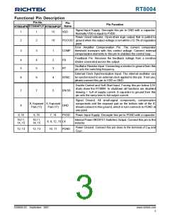
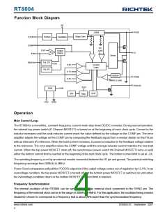
RT8004
Parameter
Switching Frequency
Symbol
Test Conditions
Min
Typ
1
Max
1.2
4
Units
MHz
MHz
MHz
mΩ
mΩ
A
R
= 309k
0.8
OSC
f
OSC
Switching Frequency Range 0.3
--
Sync Frequency Range
Switch On Resistance, High
Switch On Resistance, Low
Peak Current Limit
0.3
45
45
4
--
4
(Note 6)
R
R
75
69
5.2
2.52
0.15
--
110
100
7
I
I
= 1A
= 1A
PFET
NFET
SW
SW
I
LIM
VDD Rising
Hysteresis
2.25
--
2.7
--
V
Undervoltage Lockout Threshold
V
SW Leakage Current
EN/SS Leakage Current
Enable Threshold
--
1
μA
V
EN
= 0V, V = 5.5V
IN
--
--
1
μA
0.65
--
0.95
V
V
EN
Note 1. Stresses listed as the above “Absolute Maximum Ratings” may cause permanent damage to the device. These are for
stress ratings. Functional operation of the device at these or any other conditions beyond those indicated in the
operational sections of the specifications is not implied. Exposure to absolute maximum rating conditions for extended
periods may remain possibility to affect device reliability.
Note 2. Devices are ESD sensitive. Handling precaution recommended.
Note 3. The device is not guaranteed to function outside its operating conditions.
Note 4. θJA is measured in the natural convection at TA = 25°C on 4-layers high effective thermal conductivity test board of
JEDEC 51-7 thermal measurement standard. The case point of θJC is on the expose pad for the QFN package.
Note 5. The specifications over the -40°C to 85°C operation ambient temperature range are assured by design, characterization
and correlation with statistical process controls.
Note 6. The external synchronous frequency must be equal to 1 to 1.3 times of the internal setting frequency. The switching
frequency reange is guaranteed by design but not production tested.
DS8004-03 September 2007
www.richtek.com
7

 RICHTEK [ RICHTEK TECHNOLOGY CORPORATION ]