RT7274/79/80/81
Absolute Maximum Ratings (Note 1)
z Supply Input Voltage, VIN, VINR ------------------------------------------------------------------------------- −0.3V to 21V
z Switch Node, SW -------------------------------------------------------------------------------------------------- −0.8V to (VIN + 0.3V)
z Switch Node, SW (<10ns)---------------------------------------------------------------------------------------- −5V to 25V
z BOOT to SW, PVCC ---------------------------------------------------------------------------------------------- −0.3V to 6V
z Other Pins------------------------------------------------------------------------------------------------------------ −0.3V to 21V
z Power Dissipation, PD @ TA = 25°C
TSSOP-14 (Exposed Pad) --------------------------------------------------------------------------------------- 2.50W
SOP-8 (Exposed Pad) -------------------------------------------------------------------------------------------- 2.04W
z Package Thermal Resistance (Note 2)
TSSOP-14 (Exposed Pad), θJA --------------------------------------------------------------------------------- 40°C/W
SOP-8 (Exposed Pad), θJA --------------------------------------------------------------------------------------- 49°C/W
SOP-8 (Exposed Pad), θJC -------------------------------------------------------------------------------------- 15°C/W
z Junction Temperature Range------------------------------------------------------------------------------------- 150°C
z Lead Temperature (Soldering, 10 sec.)------------------------------------------------------------------------ 260°C
z Storage Temperature Range ------------------------------------------------------------------------------------- −65°C to 150°C
z ESD Susceptibility (Note 3)
HBM (Human Body Model)--------------------------------------------------------------------------------------- 2kV
Recommended Operating Conditions (Note 4)
z Supply Input Voltage, VIN ---------------------------------------------------------------------------------------- 4.5V to 18V
z Junction Temperature Range------------------------------------------------------------------------------------- −40°C to 125°C
z Ambient Temperature Range------------------------------------------------------------------------------------- −40°C to 85°C
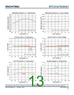
Electrical Characteristics
(VIN = 12V, TA = 25°C, unless otherwise specified)
Parameter
Supply Current
Symbol
Test Conditions
Min
Typ
Max
Unit
Supply Current (Shutdown)
Supply Current (Quiescent)
Logic Threshold
VEN = 0V
VEN = 3V, VFB = 1V
--
--
1
10
--
μA
0.7
mA
Logic High
EN Voltage
VIH
VIL
1.6
--
--
--
18
V
Logic Low
0.4
EN Pin Resistance to GND
(RT7274/81)
VEN = 12V
220
440
880
kΩ
VFB Voltage and Discharge Resistance
Feedback Threshold Voltage VFB_TH
4.5V ≤ VIN ≤ 18V
VFB = 0.8V
0.757 0.765 0.773
V
μA
Ω
Feedback Input Current
IFB
−0.1
0
0.1
VOUT Discharge Resistance RDIS
EN = 0V, VVOUT = 0.5V
--
50
100
Copyright 2013 Richtek Technology Corporation. All rights reserved.
©
is a registered trademark of Richtek Technology Corporation.
DS7274/79/80/81-01 February 2013
www.richtek.com
9

 RICHTEK [ RICHTEK TECHNOLOGY CORPORATION ]