RT6263A/B
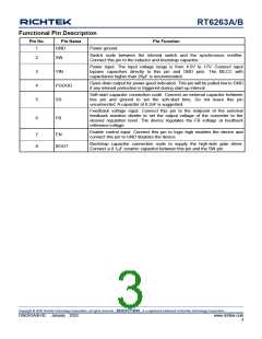
Functional Pin Description
Pin No.
Pin Name
GND
Pin Function
1
Power ground.
Switch node between the internal switch and the synchronous rectifier.
Connect this pin to the inductor and bootstrap capacitor.
2
3
4
5
SW
Power input. The input voltage range is from 4.5V to 17V. Connect input
bypass capacitors directly to this pin and GND pins. The MLCC with
capacitance higher than 20F is recommended.
VIN
Open-drain output for power-good indication. This pin will be pulled low to GND
if any internal protection is triggered during start-up interval.
PGOOD
SS
Soft-start capacitor connection node. Connect an external capacitor between
this pin and ground to set the soft-start time. Do not leave this pin
unconnected. A capacitor of 8.2nF is suggested.
Feedback voltage input. Connect this pin to the midpoint of the external
feedback resistive divider to set the output voltage of the converter to the
desired regulation level. The device regulates the FB voltage at feedback
reference voltage.
6
FB
Enable control input. Connect this pin to logic high enables the device and
connect this pin to GND disables the device.
7
8
EN
Bootstrap capacitor connection node to supply the high-side gate driver.
Connect a 0.1F ceramic capacitor between this pin and the SW pin.
BOOT
Copyright © 2020 Richtek Technology Corporation. All rights reserved.
is a registered trademark of Richtek Technology Corporation.
DS6263A/B-00 January 2020
www.richtek.com
3

 RICHTEK [ RICHTEK TECHNOLOGY CORPORATION ]