RT6236A/B
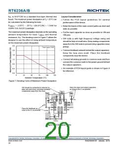
θJA, is 64.8°C/W on a standard four-layer thermal test
board. The maximum power dissipation at TA = 25°C can
be calculated by the following formula :
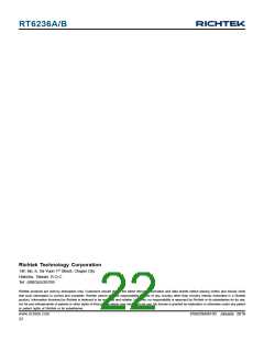
Layout Consideration
Follow the PCB layout guidelines for optimal
performance of the device.
PD(MAX) = (125°C − 25°C) / (64.8°C/W) = 1.54W for
Keep the traces of the main current paths as short and
UQFN-13JL 2x3 (FC) package
wide as possible.
The maximum power dissipation depends on the operating
ambient temperature for fixed TJ(MAX) and thermal
resistance, θJA. The derating curve in Figure 7 allows the
designer to see the effect of rising ambient temperature
on the maximum power dissipation.
Put the input capacitor as close as possible to VIN and
VIN pins.
SW node is with high frequency voltage swing and
should be kept at small area. Keep analog components
away from the SW node to prevent stray capacitive noise
pickup.
2.4
Four-Layer PCB
2.0
1.6
1.2
0.8
0.4
0.0
Connect feedback network behind the output capacitors.
Keep the loop area small. Place the feedback
components near the device.
Connect all analog grounds to common node and then
connect the common node to the power ground behind
the output capacitors.
An example of PCB layout guide is shown in Figure 8
for reference.
0
25
50
75
100
125
Ambient Temperature (°C)
Figure 7.Derating Curve of Maximum PowerDissipation
Place the input and output capacitors
as close to the IC as possible.
SW should be connected to inductor by
wide and short trace, and keep sensitive
components away from this trace.
C
BOOT
V
OUT
L
GND
C
C
IN
OUT
13
12
11
1
10
GND
EN
VIN
2
3
4
9
R1
VIN
8
FB
PGOOD
Place the feedback as
7
NC
NC
close to the IC as possible.
R2
5
6
C
SS
GND
C
PVCC
Figure 8. PCB Layout Guide
Copyright 2018 Richtek Technology Corporation. All rights reserved.
©
is a registered trademark of Richtek Technology Corporation.
www.richtek.com
20
DS6236A/B-03 January 2018

 RICHTEK [ RICHTEK TECHNOLOGY CORPORATION ]