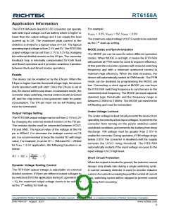
RT6158A
Marking Information
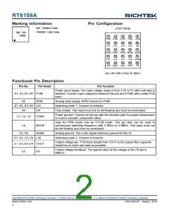
Pin Configuration
0M : Product Code
(TOP VIEW)
YMDNN : Date Code
0M YM
DNN
A1
A2
A3
A4
A5
PVIN PVIN PVIN PVIN AVIN
B1
B2
B3
B4
B5
LX1
LX1
LX1
LX1
EN
C1
C2
C3
C4
C5
PGND PGND PGND MODE AGND
D1
D2
D3
D4
D5
LX2
LX2
LX2
LX2 AGND
E1
E2
E3
E4
E5
VOUT VOUT VOUT VOUT
FB
WL-CSP-25B 2.07x2.33 (BSC)
Functional Pin Description
Pin No.
Pin Name
Pin Function
Power input supply. The input voltage range is from 2.5V to 5V after soft-start is
finished. Connect input capacitors between this pin and PGND with a wide PCB
trace.
A1, A2, A3, A4 PVIN
A5
AVIN
Analog input supply. AVIN Connect to PVIN.
B1, B2, B3, B4 LX1
Switching node 1. Connect to inductor.
B5
EN
Chip enable. This input must not be left floating and must be terminated.
Power ground. Connect to this pin with the shortest path for power transmission
to reduce parasitic component effect.
C1, C2, C3
PGND
High for PFM mode, low for FCCM mode. This pin also can be used to
synchronize switching frequency with 2.2MHz to 2.6MHz. This input must not
be left floating and must be terminated.
C4
MODE
AGND
C5, D5
Analog ground. This is the signal reference ground for the IC.
Switching node 2. Connect to inductor.
D1, D2, D3, D4 LX2
Output voltage pin. PCB trace length from VOUT to the output filter capacitor
should be as short and wide as possible.
E1, E2, E3, E4 VOUT
Output voltage feedback. The typical value of the voltage at the FB pin is
800mV.
E5
FB
Copyright 2019 Richtek Technology Corporation. All rights reserved.
©
is a registered trademark of Richtek Technology Corporation.
www.richtek.com
2
DS6158A-05 August 2019

 RICHTEK [ RICHTEK TECHNOLOGY CORPORATION ]