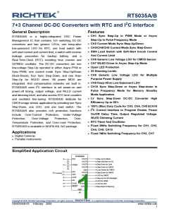
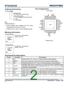
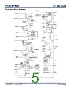
RT5035A/B
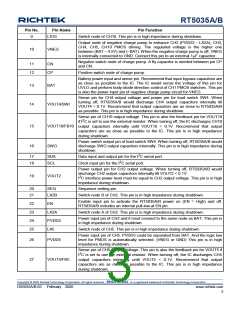
Pin No.
Pin Name
LX10
Pin Function
9
Switch node of CH10. This pin is in high impedance during shutdown.
Output node of negative charge pump to enhance CH2 (PVDD2 LX2A), CH3,
CH4, CH5, CH10 PMOS driving. The regulated voltage is the higher one
between (BAT 4.5V) and (BAT). When the negative charge pump is off, VNEG
is internally connected to GND. Connect this pin to an external 1F capacitor.
10
VNEG
Negative switch node of charge pump. A fly capacitor is needed between pin CP
and CN.
11
12
CN
CP
Positive switch node of charge pump.
Battery power input and sense pin. Recommend that input bypass capacitors are
as close as possible to the IC. The IC would sense the voltage of this pin for
UVLO and perform body-diode direction control of CH1 PMOS switches. This pin
is also the power input pin of negative charge pump circuit for VNEG.
13
14
BAT
Sense pin for CH4 output voltage and power pin for load switch SW4. When
turning off, RT5035A/B would discharge CH4 output capacitors internally till
VOUT4 < 0.1V. Recommend that output capacitors are as close to RT5035A/B
as possible. This pin is in high impedance during shutdown.
VOUT4/SWI
Sense pin of CH10 output voltage. This pin is also the feedback pin for VOUT10
if I2C is set to use the external resistor. When turning off, the IC discharges CH10
output capacitors internally until VOUT10 < 0.1V. Recommend that output
capacitors are as close as possible to the IC. This pin is in high impedance
during shutdown.
15
16
VOUT10/FB10
SWO
Power switch output pin of load switch SW4. When turning off, RT5035A/B would
discharge SWO output capacitors internally. This pin is in high impedance during
shutdown.
Data input and output pin for the I2C serial port.
Clock input pin for the I2C serial port.
17
18
SDA
SCL
Power output pin for CH2 output voltage. When turning off, RT5035A/B would
discharge CH2 output capacitors internally till VOUT2 < 0.1V.
I2C interface power level must be equal to CH2 output voltage. This pin is in high
impedance during shutdown.
19
VOUT2
20
21
SEQ
Sequence setting pin.
LX2B
Switch node B of CH2. This pin is in high impedance during shutdown.
Enable input pin to activate the RT5035A/B power on (EN = High) and off.
RT5035A/B includes an internal pull-low at EN pin.
22
23
24
25
EN
LX2A
PVDD2
LX5
Switch node A of CH2. This pin is in high impedance during shutdown.
Power input pin of CH2 and it must connect to the same node as BAT. This pin is
in high impedance during shutdown.
Switch node of CH5. This pin is in high impedance during shutdown.
Power input pin of CH5. PVDD5 could be separated from BAT. And the logic low
level for PMOS is automatically selected. (VNEG or GND) This pin is in high
impedance during shutdown.
26
PVDD5
Sense pin of CH5 Output Voltage. This pin is also the feedback pin for VOUT5 if
I2C is set to use the external resistor. When turning off, the IC discharges CH5
output capacitors internally until VOUT5 < 0.1V. Recommend that output
capacitors are as close as possible to the IC. This pin is in high impedance
during shutdown.
27
VOUT5/FB5
Copyright © 2020 Richtek Technology Corporation. All rights reserved.
is a registered trademark of Richtek Technology Corporation.
DS5035A/B-03 February 2020
www.richtek.com
3

 RICHTEK [ RICHTEK TECHNOLOGY CORPORATION ]