RFPA3800
Absolute Maximum Ratings
Parameter
Caution! ESD sensitive device.
Rating
7.5
Unit
V
Exceeding any one or a combination of the Absolute Maximum Rating conditions may
cause permanent damage to the device. Extended application of Absolute Maximum
Rating conditions to the device may reduce device reliability. Specified typical perfor-
mance or functional operation of the device under Absolute Maximum Rating condi-
tions is not implied.
Supply Voltage (V and V
) >300MHz
CC
BIAS
Supply Voltage (V and V
) <300MHz
5.5
V
CC
BIAS
Reference Current (I
)
10
mA
mA
REF
RoHS status based on EUDirective2002/95/EC (at time of this document revision).
DC Supply Current (I )
2300
C
The information in this publication is believed to be accurate and reliable. However, no
responsibility is assumed by RF Micro Devices, Inc. ("RFMD") for its use, nor for any
infringement of patents, or other rights of third parties, resulting from its use. No
license is granted by implication or otherwise under any patent or patent rights of
RFMD. RFMD reserves the right to change component circuitry, recommended appli-
cation circuitry and specifications at any time without prior notice.
CW Input Power, 2:1 Output VSWR
CW Input Power, 5:1 Output VSWR
Output Load VSWR at P3db
28
20
dBm
dBm
5:1
Operating Junction Temperature
160
°C
°C
Operating Temperature Range (T )
L
-40 to +85
Storage Temperature
-55 to +150
Class 1B
MSL 2
°C
ESD Rating: Human Body Model
Moisture Sensitvity Level
Specification
Typ.
Parameter
Unit
Condition
Min.
Max.
V
=7.0V, V
=7.0V, I =650mA
BIAS CQ
460MHz
CC
Frequency
450
460
470
23
MHz
dBm
EVB tuned for linear operation
<7.5V, load VSWR<2:1
Input Power (P
)
V
CC
IN
Gain (S21)
OIP3
18
48
dB
dBm
dBm
%
20dBm/tone, tone spacing=1MHz
EVB tuned for linear operation
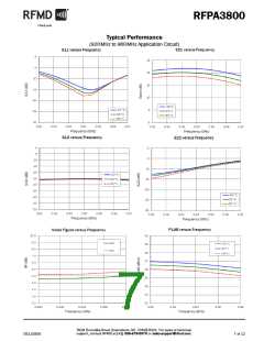
P1dB
36.7
50
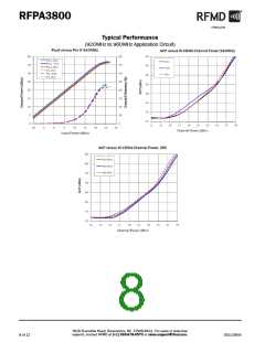
Efficiency at P3dB
At P3dB, EVB tuned for linear operation
Input Return Loss (S11)
Output Return Loss (S22)
Noise Figure
15
dB
9
dB
5
dB
WCDMA Ch Power at -65dBc ACPR
WCDMA Ch Power at -55dBc ACPR
945MHz
19.5
24.5
dBm
dBm
3GPP 3.5, Test Model 1, 64 DPCH
3GPP 3.5, Test Model 1, 64 DPCH
V
=7.0V, V
=7.0V, I =650mA
BIAS CQ
CC
Frequency
920
12
940
960
26
MHz
dBm
EVB tuned for linear operation
<7.5V, load VSWR<2:1
Input Power (P
)
V
CC
IN
Gain (S21)
OIP3
13.5
48
15.0
dB
dBm
dBm
%
945MHz
20dBm/tone, tone spacing=1MHz
EVB tuned for linear operation
At P3dB, EVB tuned for linear operation
P1dB
36
Efficiency at P3dB
45
Input Return Loss (S11)
Output Return Loss (S22)
Noise Figure
13
dB
10
dB
4
dB
WCDMA Ch Power at -65dBc ACPR
WCDMA Ch Power at -55dBc ACPR
Power Supply
19.5
24.5
dBm
dBm
3GPP 3.5, Test Model 1, 64 DPCH
3GPP 3.5, Test Model 1, 64 DPCH
Operating Current (Quiescent)
500
650
7.0
700
7.5
mA
V
At V =7.0V
CC
Operating Voltage (V
)
Max recommended collector voltage
At quiescent current, no RF
CC
Thermal Resistance (R
)
11.5
C/W
A
TH
Power Down Current
20
At V =0V.
REF
7628 Thorndike Road, Greensboro, NC 27409-9421 · For sales or technical
support, contact RFMD at (+1) 336-678-5570 or sales-support@rfmd.com.
2 of 12
DS110505

 RFMD [ RF MICRO DEVICES ]