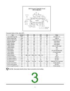
and CNTRL0 control pins. Setting CNTRL1 and CNTRL0 both high
place the unit in the receive mode. Setting CNTRL1 high and
CNTRL0 low place the unit in the ASK transmit mode (TR1100).
Setting CNTRL1 low and CNTRL0 high place the unit in the OOK
transmit mode. Setting CNTRL1 and CNTRL0 both low place the
unit in the power-down (sleep) mode. Note that the resistor driving
TXMOD must be low in the receive and power-down modes. The
PWIDTH resistor must also be low in the power down mode to mini-
mize current. CNTRL1 and CNTRL0 are CMOS compatible inputs.
These inputs must be held at a logic level; they cannot be left un-
connected.
The maximum time required to switch from the sleep mode to either
transmit mode (tSTO and tSTA) is 16 µs. Most of this time is due to the
start-up of the transmitter oscillator.
AGC Timing
The maximum AGC engage time tAGC is 5 µs after the reception of a
-30 dBm RF signal with a 1 µs envelope rise time.
The minimum AGC hold-in time is set by the value of the capacitor
at the AGCCAP pin. The hold-in time tAGH = CAGC/19.1, where tAGH is
in µs and CAGC is in pF.
Peak Detector Timing
Transceiver Event Timing
The Peak Detector attack time constant is set by the value of the ca-
pacitor at the PKDET pin. The attack time tPKA = CPKD/4167, where
tPKA is in µs and CPKD is in pF. The Peak Detector decay time con-
Transceiver event timing is summarized in Table 1. Please refer to
this table for the following discussions.
stant tPKD = 1000*tPKA
.
Turn-On Timing
Pulse Generator Timing
The maximum time tPR required for the receive function to become
operational at turn on is influenced by two factors. All receiver cir-
cuitry will be operational 5 ms after the supply voltage reaches
2.2 Vdc. The BBOUT-CMPIN coupling-capacitor is then DC stabi-
lized in 3 time constants (3*tBBC). The total turn-on time to stable re-
ceiver operation for a 10 ms power supply rise time is:
In the low data rate mode, the interval tPRI between the falling edge
of an ON pulse to the first RF amplifier and the rising edge of the
next ON pulse to the first RF amplifier is set by a resistor RPR be-
tween the PRATE pin and ground. The interval can be adjusted be-
tween 0.1 and 5 µs with a resistor in the range of 51 K to 2000 K.
The value of the RPR is given by:
tPR = 15 ms + 3*tBBC
R
PR = 404* tPRI + 10.5, where tPRI is in µs, and RPR is in kilohms
The maximum time required for either the OOK or ASK transmitter
mode to become operational is 5 ms after the supply voltage
reaches 2.2 Vdc.
In the high data rate mode normally use by the TR1100 (selected at
the PWIDTH pin), the receiver RF amplifiers operate at a nominal
50ꢀ-50ꢀ duty cycle. In this case, the period tPRC from the start of
an ON pulse to the first RF amplifier to the start of the next ON
pulse to the first RF amplifier is controlled by the PRATE resistor
over a range of 0.1 to 1.1 µs using a resistor of 11 K to 220 K. In
this case RPR is given by:
Receive-to-Transmit Timing
After turn on, the maximum time required to switch from receive to
either transmit mode is 12 µs. Most of this time is due to the start-up
of the transmitter oscillator.
Transmit-to-Receive Timing
RPR = 198* tPRC - 8.51, where tPRC is in µs and RPR is in kilohms
The maximum time required to switch from the OOK or ASK trans-
mit mode to the receive mode is 3*tBBC, where tBBC is the BBOUT-
CMPIN coupling-capacitor time constant. When the operating tem-
perature is limited to 60 oC, the time required to switch from transmit
to receive is dramatically less for short transmissions, as less
charge leaks away from the BBOUT-CMPIN coupling capacitor.
In the low data rate mode, the PWIDTH pin sets the width of the ON
pulse to the first RF amplifier tPW1 with a resistor RPW to ground (the
ON pulse width to the second RF amplifier tPW2 is set at 1.1 times
the pulse width to the first RF amplifier in the low data rate mode).
The ON pulse width tPW1 can be adjusted between 0.55 and 1 µs
with a resistor value in the range of 200 K to 390 K. The value of
RPW is given by:
Sleep and Wake-Up Timing
The maximum transition time from the receive mode to the
power-down (sleep) mode tRS is 10 µs after CNTRL1 and CNTRL0
are both low (1 µs fall time).
RPW = 404* tPW1 - 18.6, where tPW1 is in µs and RPW is in kilohms
However, when the PWIDTH pin is connected to Vcc through a 1 M
resistor, the RF amplifiers operate at a nominal 50ꢀ-50ꢀ duty cy-
cle, facilitating high data rate operation. In this case, the RF amplifi-
ers are controlled by the PRATE resistor as described above.
The maximum transition time from either transmit mode to the sleep
mode (tTOS and tTAS) is 10 µs after CNTRL1 and CNTRL0 are both
low (1 µs fall time).
LPF Group Delay
The maximum transition time tSR from the sleep mode to the receive
mode is 3*tBBC, where tBBC is the BBOUT-CMPIN coupling-capacitor
time constant. When the operating temperature is limited to 60 oC,
the time required to switch from sleep to receive is dramatically less
for short sleep times, as less charge leaks away from the BBOUT-
CMPIN coupling capacitor.
The low-pass filter group delay is a function of the filter 3 dB band-
width, which is set by a resistor RLPF to ground at the LPFADJ pin.
The minimum 3 dB bandwidth fLPF = 1445/RLPF, where fLPF is in kHz,
and RLPF is in kilohms.
The maximum group delay tFGD = 1750/fLPF = 1.21*RLPF, where tFGD
is in µs, fLPF in kHz, and RLPF in kilohms.
7

 RFM [ RF MONOLITHICS, INC ]