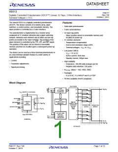
X9313
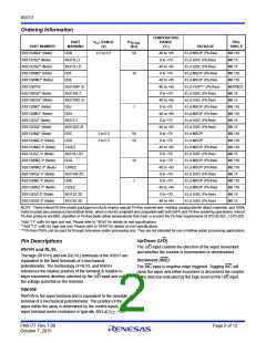
Ordering Information
TEMPERATURE
RANGE
PART
MARKING
V
RANGE
(V)
R
PKG.
DWG. #
CC
TOTAL
(k)
PART NUMBER
X9313UMIZ* (Note)
X9313USZ* (Note)
X9313USIZ* (Note)
X9313WMZ* (Note)
X9313WMIZ* (Note)
X9313WPIZ
(°C)
PACKAGE
8 Ld MSOP (Pb-free)
8 Ld SOIC (Pb-free)
8 Ld SOIC (Pb-free)
8 Ld MSOP (Pb-free)
8 Ld MSOP (Pb-free)
8 Ld PDIP*** (Pb-free)
8 Ld SOIC (Pb-free)
8 Ld SOIC (Pb-free)
8 Ld MSOP (Pb-free)
8 Ld MSOP (Pb-free)
8 Ld SOIC (Pb-free)
8 Ld SOIC (Pb-free)
8 Ld MSOP
DDB
4.5 to 5.5
50
-40 to +85
0 to +70
M8.118
M8.15
X9313U Z
X9313U ZI
DDF
-40 to +85
0 to +70
M8.15
10
M8.118
M8.118
MDP0031
M8.15
DDE
-40 to +85
-40 to +85
0 to +70
X9313WP ZI
X9313W Z
X9313WS ZI
DDJ
X9313WSZ* (Note)
X9313WSIZ* (Note)
X9313ZMZ* (Note)
X9313ZMIZ* (Note)
X9313ZSZ* (Note)
X9313ZSIZ* (Note)
X9313UMZ* (Note)
X9313UMZ-3* (Note)
X9313UMIZ-3* (Note)
X9313USZ-3* (Note)
X9313WMZ-3* (Note)
X9313WMIZ-3* (Note)
X9313WSZ-3* (Note)
X9313ZMZ-3* (Note)
X9313ZMIZ-3* (Note)
X9313ZSZ-3* (Note)
X9313ZSIZ-3* (Note)
-40 to +85
0 to +70
M8.15
1
M8.118
M8.118
M8.15
DDH
-40 to +85
0 to +70
X9313 Z
X9313ZS ZI
DDC
-40 to +85
0 to +70
M8.15
3 to 5.5
3 to 5.5
50
50
M8.118
M8.118
M8.118
M8.15
DDD
0 to +70
8 Ld MSOP
13UEZ
-40 to +85
0 to +70
8 Ld MSOP (Pb-free)
8 Ld SOIC (Pb-free)
8 Ld MSOP (Pb-free)
8 Ld MSOP (Pb-free)
8 Ld SOIC (Pb-free)
8 Ld MSOP (Pb-free)
8 Ld MSOP (Pb-free)
8 Ld SOIC (Pb-free)
8 Ld SOIC (Pb-free)
X9313U ZD
DDG
10
1
0 to +70
M8.118
M8.118
M8.15
13WEZ
-40 to +85
0 to +70
X9313W ZD
DDK
0 to +70
M8.118
M8.118
M8.15
13ZEZ
-40 to +85
0 to +70
X9313Z ZD
X9313Z ZE
-40 to +85
M8.15
NOTE: These Intersil Pb-free plastic packaged products employ special Pb-free material sets, molding compounds/die attach materials, and 100%
matte tin plate plus anneal (e3 termination finish, which is RoHS compliant and compatible with both SnPb and Pb-free soldering operations). Intersil
Pb-free products are MSL classified at Pb-free peak reflow temperatures that meet or exceed the Pb-free requirements of IPC/JEDEC J STD-020.
*Add “T1” suffix for tape and reel. Please refer to TB347 for details on reel specifications.
**Add "T2" suffix for tape and reel. Please refer to TB347 for details on reel specifications.
***Pb-free PDIPs can be used for through hole wave solder processing only. They are not intended for use in Reflow solder processing applications.
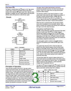
Up/Down (U/D)
Pin Descriptions
The U/D input controls the direction of the wiper movement
and whether the counter is incremented or decremented.
RH/VH and RL/VL
The high (RH/VH) and low (RL/VL) terminals of the X9313 are
Increment (INC)
equivalent to the fixed terminals of a mechanical
potentiometer. The terminology of RL/VL and RH/VH
references the relative position of the terminal in relation to
wiper movement direction selected by the U/D input and not
the voltage potential on the terminal.
The INC input is negative-edge triggered. Toggling INC will
move the wiper and either increment or decrement the counter
in the direction indicated by the logic level on the U/D input.
RW/VW
RW/VW is the wiper terminal and is equivalent to the movable
terminal of a mechanical potentiometer. The position of the
wiper within the array is determined by the control inputs. The
wiper terminal series resistance is typically 40 at V
= 5V.
CC
FN8177 Rev 7.00
October 7, 2015
Page 2 of 12

 RENESAS [ RENESAS TECHNOLOGY CORP ]