RX62Nグループ、RX621グループ
5. Electrical Characteristics
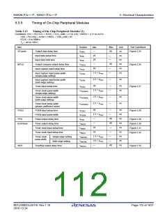
5.3.5
Timing of On-Chip Peripheral Modules
Table 5.13
Timing of On-Chip Peripheral Modules (1)
Conditions: VCC = PLLVCC = AVCC = VCC_USB = 2.7 to 3.6V, VREFH = 2.7V to AVCC
VSS = PLLVSS = AVSS = VREFL = VSS_USB = 0V
PCLK = 8 to 50MHz
Ta = -40 to +85C
Item
Symbol
tPWD
Max.
40
Unit
ns
Test Conditions
Figure 5.25
Min.
—
I/O ports
Output data delay time
Input data setup time
tPRS
25
25
—
—
ns
ns
Input data hold time
tPRH
—
40
—
ns
ns
ns
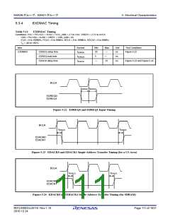
MTU2
Output compare output delay time
Input capture input setup time
tTOCD
tTICS
tTICW
Figure 5.26
20
1.5 × tPcyc
—
Input capture input pulse width
(single-edge setting)
2.5 × tPcyc
—
ns
Input capture input pulse width
(both-edge setting)
tTICW
20
—
—
ns
ns
Timer input setup time
tTCKS
Figure 5.27
1.5 × tPcyc
Timer clock pulse width
(single-edge setting)
tTCKWH/L
2.5 × tPcyc
2.5 × tPcyc
—
—
ns
ns
Timer clock pulse width
(both-edge setting)
tTCKWH/L
Timer clock pulse width
(phase coefficient mode)
tTCKWH/L
50
—
—
40
40
—
—
—
—
40
ns
ns
ns
ns
ns
ns
ns
ns
ns
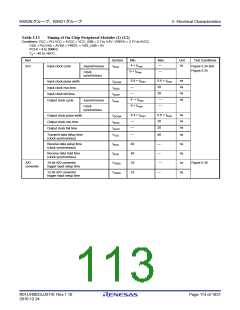
POE2
POE# input setup time
tPOES
tPOEW
tPOD
Figure 5.28
1.5 × tPcyc
POE# input pulse width
Pulse output delay time
Timer output delay time
Timer reset input setup time
Timer clock input setup time
—
PPG
Figure 5.29
Figure 5.30
Figure 5.31
Figure 5.32
—
8-bit timer
tTMOD
tTMRS
tTMCS
tTMCWH
tTMCWL
tWOVD
25
25
1.5 × tPcyc
2.5 × tPcyc
—
Timer clock
pulse width
Single-edge setting
Both-edge setting
WDT
Overflow output delay time
Figure 5.33
R01UH0033JJ0110 Rev.1.10
2010.12.24
Page 112 of 1931

 RENESAS [ RENESAS TECHNOLOGY CORP ]