M51995AP/AFP
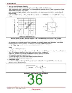
DET Circuit
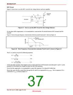
Figure 41 shows how to use the DET circuit for the voltage detector and error amplifier.
A
Detecting
voltage
C
C1
R1
R2
F/B
C2 R3
M51995A
DET
B
C4
Figure 41 How to use the DET Circuit for the Voltage Detector
For the phase shift compensation, it is recommended to connected the CR network between DET terminal and F/B
terminal.
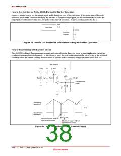
Figure 42 shows the gain-frequency characteristics between point B and point C shown in figure 41.
GAVDET
(DC Voltage gain)
G1
ω1
ω2
Log ω
Figure 42 Gain-Frequency Characteristics between Point B and C shown in Figure 41
The G1, ω1 and ω2 are given by following equations;
R3
G1 =
ω1 =
ω2 =
……………………… (12)
………………………… (13)
R1 / R2
1
C2 • R3
C1 + C2
………………… (14)
C1 • C2 • R3
At the start of the operation, there happen to be no output pulse due to F/B terminal current through C1 and C2, as the
potential of F/B terminal rises sharply just after the start of the operation.
Not to lack the output pulse, is recommended to connect the capacitor C4 as shown by broken line.
Please take notice that the current flows through the R1 and R2 are superposed to ICC(START). Not to superpose, R1 is
connected to CVCC2 as shown in figure 25.
Rev.2.00 Jun 14, 2006 page 37 of 40

 RENESAS [ RENESAS TECHNOLOGY CORP ]