M51995AP/AFP
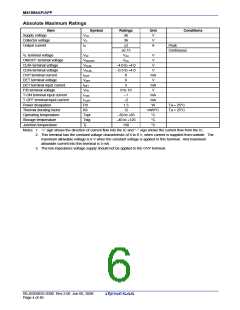
Absolute Maximum Ratings
Item
Symbol
Ratings
Unit
V
Conditions
Supply voltage
Collector voltage
Output current
VCC
36
VC
IO
36
V
±2
A
Peak
±0.15
Continuous
VF terminal voltage
VVF
VCC
V
V
ON/OFF terminal voltage
CLM−terminal voltage
CLM+terminal voltage
OVP terminal current
DET terminal voltage
DET terminal input current
F/B terminal voltage
VON/OFF
VCC
VCLM
−4.0 to +4.0
V
−
VCLM
−0.3 to +4.0
V
+
IOVP
VDET
IDET
VFB
ITON
ITOFF
Pd
8
mA
V
6
5
0 to 10
−1
mA
V
T-ON terminal input current
T-OFF terminal input current
Power dissipation
mA
mA
W
−2
1.5
Ta = 25°C
Ta > 25°C
Thermal derating factor
Operating temperature
Storage temperature
Junction temperature
Kθ
12
mW/°C
°C
Topr
Tstg
Tj
−30 to +85
−40 to +125
150
°C
°C
Notes: 1. “+” sign shows the direction of current flow into the IC and “−” sign shows the current flow from the IC.
2. This terminal has the constant voltage characteristic of 6 to 8 V, when current is supplied from outside. The
maximum allowable voltage is 6 V when the constant voltage is applied to this terminal. And maximum
allowable current into this terminal is 5 mA.
3. The low impedance voltage supply should not be applied to the OVP terminal.
REJ03D0835-0300 Rev.3.00 Jun 06, 2008
Page 4 of 40

 RENESAS [ RENESAS TECHNOLOGY CORP ]