M37161M8/MA/MF-XXXSP/FP,M37161EFSP/FP
8.10.14 OSD Output Pin Control
The OSD output pins R, G, B and OUT can also function as ports
P52–P55. Set the corresponding bit of the OSD port control register
(address 00CB16) to “0” to specify these pins as OSD output pins, or
to “1” to specify as the general-purpose port P5.
The input polarity of the HSYNC and VSYNC, and the output polarity of
signals R, G, B, OUT can be specified with the I/O polarity control
register (address 00D8.) Set bits to “0” to specify positive polarity; “1”
to specify negative polarity (refer to Figure 8.10.13).
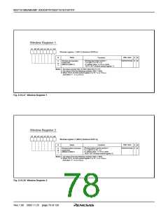
The structure of the OSD port control register is shown in Figure
8.10.29.
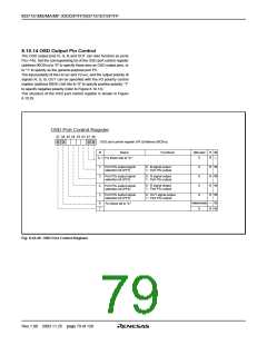
OSD Port Control Register
b7 b6 b5 b4 b3 b2 b1 b0
OSD port control register (PF) [Address 00CB16
]
0 0
0 0
R
R
B
Name
Functions
After reset
0
W
—
0, 1
Fix these bits to “0.”
2
3
4
5
Port P5
selection bit (PF2)
2
output signal
0 : B signal output
1 : Port P5 output
0
0
0
0
R
R
R
R
W
W
W
W
2
Port P5
3
output signal
0 : G signal output
1 : Port P5 output
selection bit (PF3)
3
0 : R signal output
1 : Port P5 output
Port P54 output signal
4
selection bit (PF4)
Port P5 output signal
5
0 : OUT signal output
1 : Port P5 output
selection bit (PF5)
5
6
7
Indeterminate
0
—
W
W
Fix these bit to “0.”
R
Fig. 8.10.29 OSD Port Control Register
Rev.1.00 2003.11.25 page 79 of 128

 RENESAS [ RENESAS TECHNOLOGY CORP ]