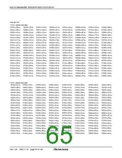
M37161M8/MA/MF-XXXSP/FP,M37161EFSP/FP
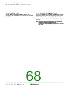
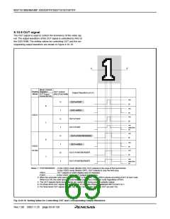
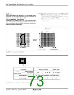
8.10.8 OUT signal
The OUT signal is used to control the luminance of the video sig-
nal. The output waveform of the OUT signal is controlled by RA3 of
the OSD RAM. The setting values for controlling OUT and the cor-
responding output waveform are shown in Figure 8.10.18.
A'
A
Block Control
Display Register i
OUT control
(RA3 of OSD RAM)
Output Waveform (A-A')
Mode
OUT Output
Control Bit (b5)
Vcc
0V
0
1
0
1
0
1
0
1
OUT=FONT
OUT=AREA
OUT=FONT
OUT=FONT
0
Vcc
0V
OSD1
Vcc
0V
1
Vcc
About 0.6Vcc
0V
Vcc
0V
OUT=FONT/BORDER
OUT=AREA
0
Vcc
OSD2
0V
CD OSD
Vcc
OUT=FONT/BORDER
OUT=FONT/BORDER
0V
1
Vcc
About 0.6Vcc
0V
Notes 1: FONT/BORDER.....In the OSD2 mode (Border ON), OUT outputs to the area of font and border.
In the OSD2 mode (Border OFF), OUT outputs to only the font area.
AREA.....................OUT outputs to entire display area of character.
FONT.....................In the OSD1 mode, OUT outputs to font area.
2: When the automatic solid space function is OFF in the OSD1 mode, AREA outputs according to bit 3 of color code.
When it is ON, the solid space is automatically output by a character code regardless of RA3.
3: The OUT signal's three-level outputs are useful only during positive polarity output.
4: For three-level OUT signal outputs, set Port P3 Direction Register (address 00C716) bit 2 to 1.
5: For three-level OUT signal outputs, set about 2 kΩ resistor between OUT pin and VSS
.
Fig. 8.10.18 Setting Value for Controlling OUT and Corresponding Output Waveform
Rev.1.00 2003.11.25 page 69 of 128

 RENESAS [ RENESAS TECHNOLOGY CORP ]