M37161M8/MA/MF-XXXSP/FP,M37161EFSP/FP
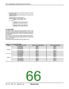
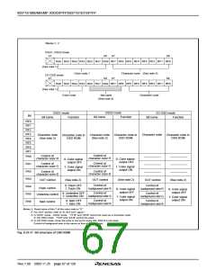
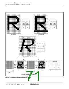
Blocks 1, 2
OSD1, OSD2 mode
b7
b0
b7
b0
RA6 RA5 RA4 RA3 RA2 RA1 RA0 RF7 RF6 RF5 RF4 RF3 RF2 RF1 RF0
(See note 1)
Color code 1
Character code (See note 3)
CD OSD mode
b7
b0
b7
b0
RA6 RA5 RA4 RA3 RA2 RA1 RA0 RF7 RF6 RF5 RF4 RF3 RF2 RF1 RF0
(See note 1)
Color code
Not used
Character code
(See note 4)
OSD2 mode
CD OSD mode
OSD1 mode
Function
Bit
Function
Bit name
Bit name
Bit name
Function
RF0
RF1
RF2
RF3
RF4
RF5
RF6
RF7
Character code
Character code
(See note 3)
Character code in
OSD ROM
Character code in
OSD ROM
Character code
(See note 3)
Character code in
OSD ROM
Control of
Control of
RA0
RA1
RA2
RA3
RA4
RA5
RA6
character color R
character color R
0: Color signal
output OFF
0: Color signal
output OFF
Control of
character color G
Control of
character color G
1: Color signal
output ON
1: Color signal
output ON
Control of
character color B
Control of
character color B
OUT control
(See note 2)
OUT control
(See note 2)
OUT control
(See note 2)
Control of
background color R
0: Flash OFF
1: Flash ON
Control of
Flash control
background color R
0: Color signal
output OFF
0: Color signal
output OFF
Control of
background color G
0: Underline OFF
1: Underline ON
Control of
Underline control
background color G
1: Color signal
output ON
1: Color signal
output ON
Control of
background color B
0: Italic OFF
1: Italic ON
Control of
Italic control
background color B
Notes 1: Read value of bits 7 of the color code is “0.”
2:
3:
For OUT control, refer to “8.10.8 OUT signal.”
In OSD1 mode , OSD2 mode, “7F16” and “8016” cannot be used as a character code.
In CD OSD mode, “1516” and “2A16” cannot be used.
4: In CD OSD mode, since the color is set up for every dot, RA2-0 is not used.
Control of background color is the same as that of OSD2 mode.
Fig. 8.10.17 Bit structure of OSD RAM
Rev.1.00 2003.11.25 page 67 of 128

 RENESAS [ RENESAS TECHNOLOGY CORP ]