HD74HC14
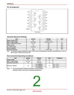
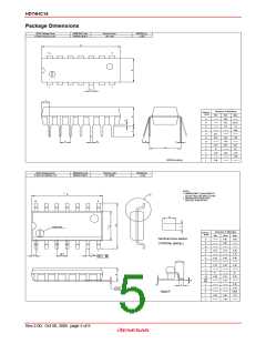
Pin Arrangement
1A
1Y
1
2
3
4
5
6
7
14 VCC
13 6A
12 6Y
11 5A
10 5Y
2A
2Y
3A
3Y
9
8
4A
4Y
GND
(Top view)
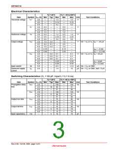
Absolute Maximum Ratings
Item
Supply voltage range
Input / Output voltage
Input / Output diode current
Output current
Symbol
Ratings
Unit
V
VCC
Vin, Vout
IIK, IOK
IO
–0.5 to 7.0
–0.5 to VCC +0.5
±20
V
mA
mA
mA
mW
°C
±25
VCC, GND current
ICC or IGND
PT
±50
Power dissipation
500
Storage temperature
Tstg
–65 to +150
Note: The absolute maximum ratings are values, which must not individually be exceeded, and furthermore, no two of
which may be realized at the same time.
Recommended Operating Conditions
Item
Supply voltage
Symbol
VCC
Ratings
2 to 6
Unit
V
Conditions
Input / Output voltage
Operating temperature
VIN, VOUT
Ta
0 to VCC
V
–40 to 85
°C
0 to unlimited
0 to unlimited
0 to unlimited
VCC = 2.0 V
VCC = 4.5 V
CC = 6.0 V
Input rise / fall time*1
tr, tf
ns
V
Note: 1. This item guarantees maximum limit when one input switches.
Waveform: Refer to test circuit of switching characteristics.
Rev.2.00, Oct 06, 2005 page 2 of 6

 RENESAS [ RENESAS TECHNOLOGY CORP ]