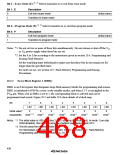
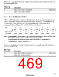
Bits 7 to 0—Large Block 7 to 0 (LB7 to LB0): These bits select large blocks (LB7 to LB0) to be
programmed and erased.
Bits 7 to 0:
LB7 to LB0
Description
0
1
Block (LB7 to LB0) is not selected
Block (LB7 to LB0) is selected
(Initial value)
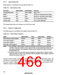
20.2.3
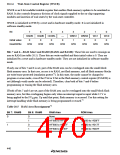
Erase Block Register 2 (EBR2)
EBR2 is an 8-bit register that designates small flash-memory blocks for programming and erasure.
EBR2 is initialized to H'00 by a reset, in the standby modes, and when 12 V is not applied to the
FVPP pin. When a bit in EBR2 is set to 1, the corresponding block is selected and can be
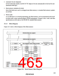
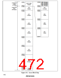
programmed and erased. Figure 20.2 and table 20.6 show a block map.
Bit
7
SB7
0
6
SB6
0
5
SB5
0
4
SB4
0
3
SB3
0
2
SB2
0
1
SB1
0
0
SB0
0
Initial value*
Read/Write
R/W*
R/W*
R/W*
R/W*
R/W*
R/W*
R/W*
R/W*
Note: * The initial value is H'00 in modes 2 and 3 (on-chip ROM enabled). In mode 1 (on-chip ROM
disabled), this register cannot be modified and always reads H'FF.
For information on accessing this register, refer to in section 20.7, Flash Memory
Programming and Erasing Precautions (11).
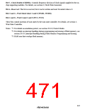
Bits 7 to 0—Small Block 7 to 0 (SB7 to SB0): These bits select small blocks (SB7 to SB0) to be
programmed and erased.
Bits 7 to 0:
SB7 to SB0
Description
0
1
Block (SB7 to SB0) is not selected
Block (SB7 to SB0) is selected
(Initial value)
439

 RENESAS [ RENESAS TECHNOLOGY CORP ]