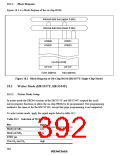
18.3
PROM Programming
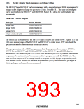
The write, verify, and other sub-modes of the writer mode are selected as shown in table 18.4.
Table 18.4 Selection of Sub-Modes in Writer Mode
Sub-Mode
Write
CE
OE
PGM
Low
VPP
VPP
VPP
VPP
VCC
VCC
VCC
VCC
EO7 to EO0
Data input
EA16 to EA0
Low
Low
High
Low
Address input
Address input
Address input
Verify
High
Data output
High impedance
Programming
inhibited
Low
Low
High
High
Low
High
Low
High
Low
High
Low
High
Legend:
VPP: VPP level
VCC: VCC level
The H8/3337Y and H8/3334Y PROM have the same standard read/write specifications as the
HN27C101 EPROM. Page programming is not supported, however, so do not select page
programming mode. PROM programmers that provide only page programming cannot be used.
When selecting a PROM programmer, check that it supports a byte-at-a-time high-speed
programming mode. Be sure to set the address range to H'0000 to H'F77F for the H8/3337Y, and
to H'0000 to H'7FFF for the H8/3334Y.
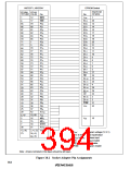
18.3.1
Programming and Verification
An efficient, high-speed programming procedure can be used to program and verify PROM data.
This procedure programs data quickly without subjecting the chip to voltage stress and without
sacrificing data reliability. It leaves the data H'FF in unused addresses.
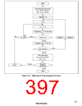
Figure 18.5 shows the basic high-speed programming flowchart.
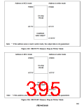
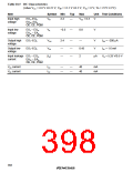
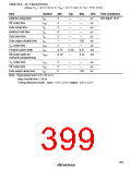
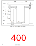
Tables 18.5 and 18.6 list the electrical characteristics of the chip in writer mode. Figure 18.6
shows a program/verify timing chart.
366

 RENESAS [ RENESAS TECHNOLOGY CORP ]