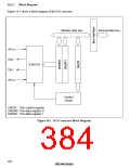
16.3
Operation
The D/A converter module has two built-in D/A converter circuits that can operate independently.
D/A conversion is performed continuously whenever enabled by the D/A control register. When a
new value is written in DADR0 or DADR1, conversion of the new value begins immediately. The
converted result is output by setting the DAOE0 or DAOE1 bit to 1.
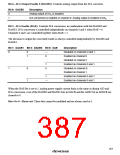
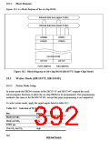
An example of conversion on channel 0 is given next. Figure 16.2 shows the timing.
1. Software writes the data to be converted in DADR0.
2. D/A conversion begins when the DAOE0 bit in DACR is set to 1. After a conversion delay,
analog output appears at the DA0 pin. The output value is AVCC × (DADR0 value)/256.
This output continues until a new value is written in DADR0 or the DAOE0 bit is cleared to 0.
3. If a new value is written in DADR0, conversion begins immediately. Output of the converted
result begins after the conversion delay time.
4. When the DAOE0 bit is cleared to 0, DA0 becomes an input pin.
DADR0
write cycle
DACR
write cycle
DADR0
write cycle
DACR
write cycle
ø
Address
DADR0
Conversion data (1)
Conversion data (2)
DAOE0
DA0
Conversion result (2)
Conversion result (1)
High-impedance state
tDCONV
tDCONV
tDCONV: D/A conversion time
Figure 16.2 D/A Conversion (Example)
358

 RENESAS [ RENESAS TECHNOLOGY CORP ]