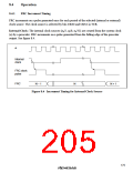
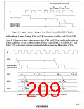
ICR upper byte read cycle
T1 T2 T3
ø
Input at FTI pin
Internal input
capture signal
Figure 8.9 Input Capture Timing (1-State Delay Due to ICRA/B/C/D Read)
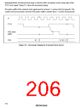
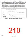
Buffered Input Capture Timing: ICRC and ICRD can operate as buffers for ICRA and ICRB.
Figure 8.10 shows how input capture operates when ICRA and ICRC are used in buffer mode and
IEDGA and IEDGC are set to different values (IEDGA = 0 and IEDGC = 1, or IEDG A = 1 and
IEDGC = 0), so that input capture is performed on both the rising and falling edges of FTIA.
ø
FTIA
Internal input
capture signal
FRC
n
n + 1
N
N + 1
M
n
N
ICRA
ICRC
n
m
M
M
n
Figure 8.10 Buffered Input Capture with Both Edges Selected
179

 RENESAS [ RENESAS TECHNOLOGY CORP ]