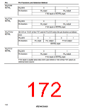
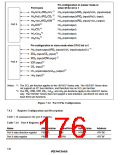
Pin configuration in master mode or
when STAC bit is 1
Port 8 pins
P86/SCK1/IRQ5/SCL*1 P86 (input/output)/IRQ5 (input)/SCK1 (input/output)
*2
P85/RxD1/IRQ4/CS2
P85 (input/output)/IRQ4 (input)/RxD1 (input)
P84/TxD1/IRQ3/IOW *2 P84 (input/output)/IRQ3 (input)/TxD1 (output)
P83/IOR*2
P83 (input/output)
P82 (input/output)
P81 (input/output)
P80 (input/output)
Port 8
*2
P82/CS1
*2
P81/GA20
*2
P80/HA0
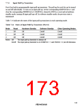
Pin configuration in slave mode when STAC bit is 0
P86 (input/output)/IRQ5 (input)/SCK1 (input/output)/SCL*1
IRQ4 (input)/CS2 (input)*2
IRQ3 (input)/IOW (input)*2
IOR (input)*2
Port 8
CS1 (input)*2
P81 (input/output)/GA20 (output)*2
HA0 (input)*2
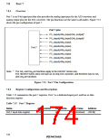
Notes: *1 The SCL pin function applies to the H8/3337 Series only. The H8/3397 Series does
not support an I2C bus interface, and therefore has no SCL pin function.
*2 The CS2, IOW, IOR, CS1, GA20, and HA0 pin functions apply to the H8/3337 Series
only. The H8/3397 Series does not support a host interface, and theref ore does not
have these pin functions.
Figure 7.16 Port 8 Pin Configuration
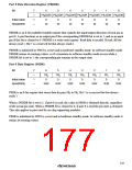
7.9.2
Register Configuration and Descriptions
Table 7.16 summarizes the port 8 registers.
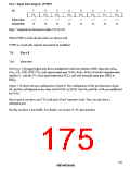
Table 7.16 Port 8 Registers
Name
Abbreviation
P8DDR
Read/Write
Initial Value
H'80
Address
H'FFBD
H'FFBF
Port 8 data direction register
Port 8 data register
W
P8DR
R/W
H'80
146

 RENESAS [ RENESAS TECHNOLOGY CORP ]