Bank Active: The synchronous DRAM bank function is used to support high-speed accesses to
the same row address. When the RASD bit in MCR is 1, read/write command accesses are
performed using commands without auto-precharge (READ, WRIT). In this case, precharging is
not performed when the access ends. When accessing the same row address in the same bank, it is
possible to issue the READ or WRIT command immediately, without issuing an ACTV command,
in the same way as in the RAS down state in DRAM fast page mode. As synchronous DRAM is
internally divided into two or four banks, it is possible to activate one row address in each bank. If
the next access is to a different row address, a PRE command is first issued to precharge the
relevant bank, then when precharging is completed, the access is performed by issuing an ACTV
command followed by a READ or WRIT command. If this is followed by an access to a different
row address, the access time will be longer because of the precharging performed after the access
request is issued.
In a write, when auto-precharge is performed, a command cannot be issued for a period of Trwl +
Tpc cycles after issuance of the WRITA command. When bank active mode is used, READ or
WRIT commands can be issued successively if the row address is the same. The number of cycles
can thus be reduced by Trwl + Tpc cycles for each write. The number of cycles between issuance
of the precharge command and the row address strobe command is determined by the TPC bits in
MCR.
Whether faster execution speed is achieved by use of bank active mode or by use of basic access is
determined by the probability of accessing the same row address (P1), and the average number of
cycles from completion of one access to the next access (Ta). If Ta is greater than Tpc, the delay
due to the precharge wait when writing is imperceptible. In this case, the access speed for bank
active mode and basic access is determined by the number of cycles from the start of access to
issuance of the read/write command: (Tpc + Trcd) × (1 – P1) and Trcd, respectively.
There is a limit on Tras, the time for placing each bank in the active state. If there is no guarantee
that there will not be a cache hit and another row address will be accessed within the period in
which this value is maintained by program execution, it is necessary to set auto-refresh and set the
refresh cycle to no more than the maximum value of Tras. In this way, it is possible to observe the
restrictions on the maximum active state time for each bank. If auto-refresh is not used, measures
must be taken in the program to ensure that the banks do not remain active for longer than the
prescribed time.
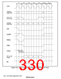
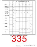
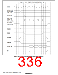
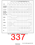
A burst read cycle without auto-precharge is shown in figure 10.19, a burst read cycle for the same
row address in figure 10.20, and a burst read cycle for different row addresses in figure 10.21.
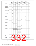
Similarly, a burst write cycle without auto-precharge is shown in figure 10.22, a burst write cycle
for the same row address in figure 10.23, and a burst write cycle for different row addresses in
figure 10.24.
Rev. 5.00, 09/03, page 289 of 760

 RENESAS [ RENESAS TECHNOLOGY CORP ]