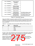
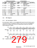
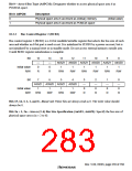
IC Memory Card Interface
Pin Signal I/O Function
I/O Card Interface
I/O Function
Signal
SH7709S Pin
61 REG
62 BVD2
63 BVD1
I
Attribute memory
space select
REG
I
Attribute memory
space select
—
O
O
Battery voltage
detection
SPKR
O
O
Digital voice signal —
Battery voltage
detection
STSCHG
Card state
change
—
64 D8
I/O Data
I/O Data
I/O Data
D8
I/O Data
I/O Data
I/O Data
D8
D9
D10
—
65 D9
D9
66 D10
67 CD2
68 GND
D10
CD2
GND
O
Card detection
Ground
O
Card detection
Ground
—
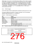
10.2
BSC Registers
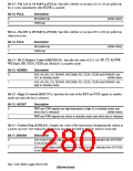
10.2.1 Bus Control Register 1 (BCR1)
Bus control register 1 (BCR1) is a 16-bit readable/writable register that sets the functions and bus
cycle state for each area. It is initialized to H'0000 by a power-on reset, but is not initialized by a
manual reset or in standby mode. Do not access external memory outside area 0 until BCR1
register initialization is complete.
Bit:
15
PULA
0
14
13
12
11
10
9
8
PULD HIZMEM HIZCNT ENDIAN A0BST1 A0BST0 A5BST1
*
Initial value:
R/W:
0
0
0
0/1
R
0
0
0
R/W
R/W
R/W
R/W
R/W
R/W
R/W
Bit:
7
6
5
4
3
2
1
0
A5BST0 A6BST1 A6BST0 DRAM DRAM DRAM A5 PCM A6 PCM
TP2
TP1
TP0
Initial value:
R/W:
0
0
0
0
0
0
0
0
R/W
R/W
R/W
R/W
R/W
R/W
R/W
R/W
Note: * Samples the value of the external pin (MD5) designating the endian in a power-on reset.
Rev. 5.00, 09/03, page 235 of 760

 RENESAS [ RENESAS TECHNOLOGY CORP ]