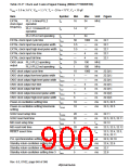
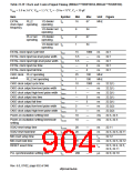
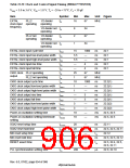
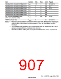
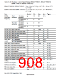
Table 22.29 Clock and Control Signal Timing (HD6417750BP200M, HD6417750SBP200)
VDDQ = 3.0 to 3.6 V, VDD = 1.5 V, Ta = –20 to +75°C, CL = 30 pF
Item
Symbol
Min
Max
Unit Figure
EXTAL
clock input operating
frequency
PLL2
1/2 divider
operating
fEX
16
67
MHz
1/2 divider not fEX
operating
8
2
1
34
67
34
PLL2 not
operating
1/2 divider
operating
fEX
1/2 divider not fEX
operating
EXTAL clock input cycle time
tEXcyc
15
3.5
3.5
—
—
25
1
1000
—
ns
22.1
22.1
22.1
22.1
22.1
EXTAL clock input low-level pulse width tEXL
EXTAL clock input high-level pulse width tEXH
ns
—
ns
EXTAL clock input rise time
EXTAL clock input fall time
CKIO clock PLL2 operating
tEXr
tEXf
4
ns
4
ns
fOP
100
100
1000
—
MHz
MHz
ns
output
PLL2 not operating
fOP
CKIO clock output cycle time
tcyc
10
1
22.2(1)
22.2(1)
22.2(1)
22.2(1)
22.2(1)
22.2(2)
22.2(2)
22.3, 22.5
22.3, 22.5
CKIO clock output low-level pulse width
tCKOL1
ns
CKIO clock output high-level pulse width tCKOH1
1
—
ns
CKIO clock output rise time
tCKOr
tCKOf
tCKOL2
—
—
3
3
ns
CKIO clock output fall time
3
ns
CKIO clock output low-level pulse width
—
ns
CKIO clock output high-level pulse width tCKOH2
3
—
ns
Power-on oscillation settling time
tOSC1
10
10
—
ms
ms
Power-on oscillation settling time/mode
settling
tOSCMD
—
SCK2 reset setup time
SCK2 reset hold time
MD reset setup time
MD reset hold time
5(6(7 assert time
tSCK2RS
tSCK2RH
tMDRS
20
20
3
—
—
—
—
—
ns
ns
tcyc
ns
tcyc
22.11
22.3, 22.5, 22.11
22.12
tMDRH
20
20
22.3, 22.5, 22.12
tRESW
22.3, 22.4, 22.5,
22.6, 22.11
PLL synchronization settling time
tPLL
200
—
µs
22.9, 22.10
Rev. 6.0, 07/02, page 852 of 986

 RENESAS [ RENESAS TECHNOLOGY CORP ]