13.3.9 Byte Control SRAM Interface
The byte control SRAM interface is a memory interface that outputs a byte select strobe (:(Q) in
both read and write bus cycles. It has 16 bit data pins, and can be connected to SRAM which has
an upper byte select strobe and lower byte select strobe function such as UB and LB.
Areas 1 and 4 can be designated as byte control SRAM interface. However, when these areas are
set to MPX mode, MPX mode has priority.
The byte control SRAM interface write timing is the same as for the normal SRAM interface.
In read operations, the :(Q pin timing is different. In a read access, only the :( signal for the
byte being read is asserted. Assertion is synchronized with the fall of the CKIO clock, as for the
:( signal, while negation is synchronized with the rise of the CKIO clock, using the same timing
as the 5' signal.
In 32-byte transfer such as a cache fill or copy-back, a total of 32 bytes are transferred
consecutively according to the set bus width. The first access is performed on the data for which
there was an access request, and the remaining accesses are performed on the data at the 32-byte
boundary. The bus is not released during this period.
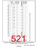
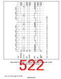
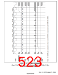
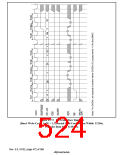
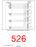
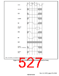
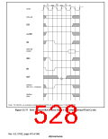
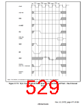
Figure 13.73 shows an example of byte control SRAM connection to the SH7750, and figures
13.74 to 13.76 show examples of byte control SRAM read cycle.
Rev. 6.0, 07/02, page 473 of 986

 RENESAS [ RENESAS TECHNOLOGY CORP ]