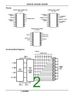
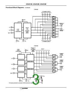
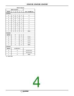
CD4051B, CD4052B, CD4053B
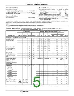
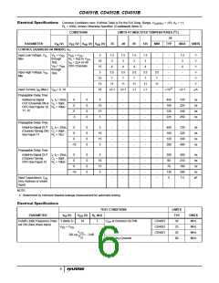
Electrical Specifications Common Conditions Here: If Whole Table is For the Full Temp. Range, V
= ±5V, A = +1,
SUPPLY
V
R
= 100Ω, Unless Otherwise Specified (Continued) (Note 3)
L
o
CONDITIONS
LIMITS AT INDICATED TEMPERATURES ( C)
25
PARAMETER
V
(V)
V
C
(V)
V
(V)
V
(V)
-55
-40
85
125
MIN
TYP
MAX
UNITS
IS
EE
SS
DD
CONTROL (ADDRESS OR INHIBIT), V
Input Low Voltage, V
Max
,
V
= V
V
R
= V ,
SS
= 1kΩ to V ,
< 2µA on All
5
1.5
3
1.5
3
1.5
3
1.5
3
-
-
-
-
-
-
-
-
1.5
V
V
IL
IL
DD
EE
through
1kΩ;
V
L
SS
10
3
I
IS
= V
OFF Channels
IH
DD
15
5
4
4
4
4
-
4
V
through
Input High Voltage, V
Min
,
3.5
7
3.5
7
3.5
7
3.5
7
3.5
7
-
V
IH 1kΩ
10
15
18
-
-
V
11
±0.1
11
±0.1
11
±1
11
±1
11
-
V
-5
Input Current, I (Max)
IN
V
= 0, 18
±10
±0.1
µA
IN
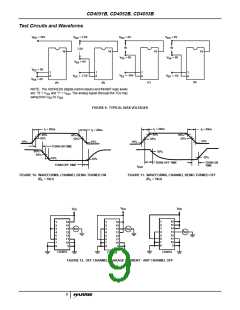
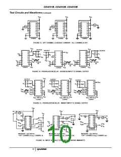
Propagation Delay Time:
Address-to-Signal
OUT (Channels ON or
OFF) See Figures 10,
11, 14
t , t = 20ns,
0
0
0
5
10
15
5
-
-
-
-
-
-
-
-
-
-
-
-
-
-
-
-
-
-
-
-
450
160
120
225
720
320
240
450
ns
ns
ns
ns
r
f
C
= 50pF,
L
L
0
0
0
R
= 10kΩ
0
-5
Propagation Delay Time:
Inhibit-to-Signal OUT t , t = 20ns,
0
0
0
0
0
0
5
10
15
5
-
-
-
-
-
-
-
-
-
-
-
-
-
-
-
-
-
-
-
-
400
160
120
200
720
320
240
400
ns
ns
ns
ns
r
f
(Channel Turning ON)
See Figure 11
C
R
= 50pF,
= 1kΩ
L
L
0
-10
Propagation Delay Time:
Inhibit-to-Signal OUT t , t = 20ns,
0
0
0
0
0
0
5
10
15
5
-
-
-
-
-
-
-
-
-
-
-
-
-
-
-
-
-
-
-
-
-
-
-
-
-
200
90
70
130
5
450
210
160
300
7.5
ns
ns
ns
ns
pF
r
f
(Channel Turning
OFF) See Figure 15
C
R
= 50pF,
= 10kΩ
L
L
0
-10
Input Capacitance, C
IN
(Any Address or Inhibit
Input)
NOTE:
2. Determined by minimum feasible leakage measurement for automatic testing.
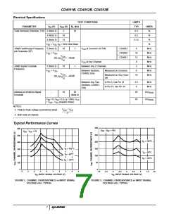
Electrical Specifications
TEST CONDITIONS
LIMITS
PARAMETER
V
(V)
V
(V)
R
(kΩ)
L
TYP
30
UNITS
IS
DD
Cutoff (-3dB) Frequency Chan- 5 (Note 3)
nel ON (Sine Wave Input)
10
1
V
at Common OUT/IN
at Any Channel
CD4053
CD4052
CD4051
MHz
MHz
MHz
MHz
OS
V
EE
= V
,
25
SS
V
20
OS
-----------
20Log
= –3dB
V
IS
V
60
OS
6

 RENESAS [ RENESAS TECHNOLOGY CORP ]