APPENDIX
Appendix 2. Control registers
✽✽Timer mode
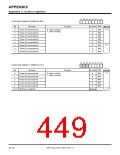
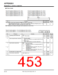
Timer A0 register (Addresses 4716, 4616)
Timer A1 register (Addresses 4916, 4816)
Timer A2 register (Addresses 4B16, 4A16)
Timer A3 register (Addresses 4D16, 4C16)
Timer A4 register (Addresses 4F16, 4E16)
Timer A5 register (Addresses C716, C616)
Timer A6 register (Addresses C916, C816)
Timer A7 register (Addresses CB16, CA16)
Timer A8 register (Addresses CD16, CC16)
Timer A9 register (Addresses CF16, CE16)
(b15)
b7
(b8)
b0
b7
b0
Bit
Function
Any value in the range from “000016” to “FFFF16” can be set.
At reset R/W
Reference
7-12
15 to 0
Undefined RW
Assuming that the set value = n, the counter divides the count source frequency by (n + 1).
When reading, the register indicates the counter value.
Note: Reading from or writing to this register must be performed in a unit of 16 bits.
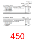
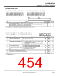
Timer Ai mode register (i = 0 to 4) (Addresses 5616 to 5A16)
Timer Ai mode register (i = 5 to 9) (Addresses D616 to DA16)
b7 b6 b5 b4 b3 b2 b1 b0
0
0 0
Function
Reference
Bit
0
Bit name
At reset R/W
b1 b0
7-12
9-12
9-23
10-15
0
0
0
RW
RW
RW
Operating mode select bits
0 0 : Timer mode
1
0 : No pulse output
7-16
2
Pulse output function select bit
Gate function select bits
(TAiOUT pin functions as a programmable I/O port
pin.)
1 : Pulse output
(TAiOUT pin functions as a pulse output pin.)
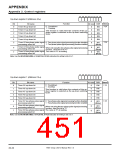
b4 b3
3
4
0
0
RW
RW
7-15
0 0 :
0 1 :
No gate function
(TAiIN pin functions as a programmable I/O
port pin.)
1 0 :
Gate function
(Counter is active only while TAiIN pin’s in-
put signal is at “L” level.)
Gate function
1 1 :
(Counter is active only while TAiIN pin’s in-
put signal is at “H” level.)
Fix this bit to “0” in timer mode.
5
6
7
0
0
0
RW
RW
RW
Count source select bits
See Table 7.2.3.
7-5
7905 Group User’s Manual Rev.1.0
20-22

 RENESAS [ RENESAS TECHNOLOGY CORP ]