POWER SAVING FUNCTIONS
16.3 Stop of oscillation circuit, 16.4 Pin VREF disconnection
16.3 Stop of oscillation circuit
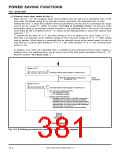
When a stable clock externally generated is input to pin XIN, power consumption can be saved by setting
the external clock input select bit to “1” to stop the drive circuit for oscillation between pins XIN and XOUT
.
(See Figure 16.1.1.) At this time, the output level at pin XOUT is fixed to “H.” Also, if the system clock select
bit (bit 5 at address BC16) = “0,” the watchdog timer is not used when the stop mode is terminated owing
to an interrupt request occurrence; therefore, the microcomputer can start instruction execution just after
termination of the stop mode. When the system clock select bit = “1,” in this case, the watchdog timer is
used.
16.4 Pin VREF disconnection
When the A-D converter is not used, power consumption can be saved by setting the VREF connection select
bit (See Figure 16.4.1) to “1.” It is because the reference voltage input pin (VREF) is disconnected from the
ladder resistors of the A-D converter, and there is no current flow between them.
When the VREF connection select bit has been cleared from “1” (VREF disconnected) to “0” (VREF connected),
be sure to start the A-D conversion after an interval of 1 µs or more has elapsed.
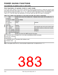
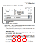
b7 b6 b5 b4 b3 b2 b1 b0
A-D control register 1 (Address 1F16
)
0
Bit
0
Bit name
At reset
1
Function
R/W
RW
Single sweep mode/Repeat sweep mode 0
A-D sweep pin select bits
b1 b0
(Valid in the single sweep mode,
repeat sweep mode 0, and
0 0 : Pins AN0 and AN1 (2 pins)
0 1 : Pins AN0 to AN3 (4 pins)
1 0 : Pins AN0 to AN5 (6 pins)
repeat sweep mode 1.)
(Note 1)
1 1 : Pins AN0 to AN7 (8 pins) (Note 2)
RW
1
1
Repeat sweep mode 1
b1 b0
(Note 3)
0 0 : Pin AN0 (1 pin)
0 1 : Pins AN0 and AN1 (2 pins)
1 0 : Pins AN0 to AN2 (3 pins)
1 1 : Pins AN0 to AN3 (4 pins)
A-D operation mode select bit 1
(Used in the repeat sweep mode 0
and repeat sweep mode 1.)(Note 4)
0 : Repeat sweep mode 0
1 : Repeat sweep mode 1
RW
RW
0
2
3
Resolution select bit
0
0
0 : 8-bit resolution mode
1 : 10-bit resolution mode
A-D conversion frequency (φAD) select bit 1
Fix this bit to “0.”
4
5
6
RW
RW
See Table 12.2.1.
0
0
VREF connection select bit (Note 5) 0 : Pin VREF is connected.
RW
1 : Pin VREF is disconnected.
–
The value is “0” at reading.
7
0
Notes 1: These bits are invalid in the one-shot and repeat modes. (They may be either “0” or “1.”)
2: When using pin AN7, be sure that the D-A0 output enable bit (bit 0 at address 9616) = “0” (output disabled).
3: Be sure to select the frequently-used analog input pins in the repeat sweep mode 1.
4: Fix this bit to “0” in the one-shot mode, repeat mode, and single sweep mode.
5: When this bit is cleared from “1” to “0,” be sure to start the A-D conversion after an interval of 1 µs or more has elapsed.
6: Writing to each bit of the A-D control register 1 must be performed while the A-D converter halts, regardless of the A-D
operation mode.
Fig. 16.4.1 Structure of A-D control register 1
7905 Group User’s Manual Rev.1.0
16-7

 RENESAS [ RENESAS TECHNOLOGY CORP ]