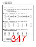
A-D CONVERTER
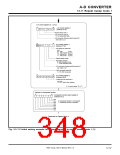
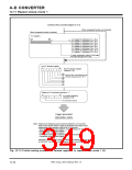
[Precautions for A-D converter]
[Precautions for A-D converter]
1. Be sure to clear the VREF connection select bit to “0.”
2. Writing to the following must be performed before a trigger is generated (in other words, while the A-D
converter halts); this must be done independent of the operation mode of the A-D converter.
• Each bit of the A-D control register 0, except writing of “0” to bit 6
• Each bit of the A-D control register 1
• Each bit of the A-D control register 2
• A-D register i (when the comparator function is selected)
• Comparator function select register 0
• Comparator function select register 1
• Comparator result register 0
• Comparator result register 1
Especially, when any instruction which clears the VREF connection select bit from “1” to “0” has been
executed (in other words, the resistor ladder network is connected with pin VREF by this instruction), an
interval of 1 µs or more must be elapsed before occurrence of a trigger.
3. When using pins AN
0
to AN , regardless of the A-D operation mode, be sure to fix bit 3 of the analog
7
input pin select bits 1 (bits 3 to 0 at address DB16) to “0.”
4. Pins AN to AN11 can be used only in the one-shot mode or repeat mode.
8
5. The analog input pin select bits 0 (bits 2 to 0 at address 1E16) and the analog input pin select bits 1 (bits
3 to 0 at address DB16) must be specified again if the user switches the operation mode to the one-shot
mode or repeat mode after the operation is performed in the single sweep mode, repeat sweep mode 0,
or repeat sweep mode 1.
6. Reading from A-D register i (when the comparator function is selected) must be performed before occurrence
of a trigger (in other words, while the A-D converter halts.). The value undefined at reading.
7. When using pin AN
When using pin AN
7
8
, be sure that the D-A
, be sure that the D-A
0
1
output enable bit (bit 0 at address 9616) = “0” (output disabled).
output enable bit (bit 1 at address 9616) = “0” (output disabled).
Also, be sure not to use pin CTS
When using pin AN , be sure not to use pin CTS
When using pin AN10, be sure not to use pin R
When using pin AN11, be sure not to use pin T D .
2
/RTS
2
.
9
2
/CLK .
2
X
D2.
X
2
8. Setting of bit 3 of the analog input pin select bits 1 (bits 3 to 0 at address DB16) to “1” invalidates the
analog input pin select bits 0 (bits 2 to 0 at address 1E16).
9. Refer to section “Appendix 7. Countermeasures against noise” when using the A-D converter.
7905 Group User’s Manual Rev.1.0
12-40

 RENESAS [ RENESAS TECHNOLOGY CORP ]