TIMER B
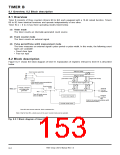
8.2 Block description
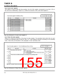
8.2.5 Port P2 direction register, Port P5 direction register
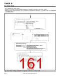
The input pins of timer Bi are multiplexed with port P5 pins. By using the TB0IN/TB1IN/TB2IN pin select bit
(see Figure 8.2.5.), pin TB0IN/TB1IN/TB2IN can be allocated to the corresponding port P2 pin.
When using pins P5
5
(P2
4
)/TB0IN, P5
6
(P2
5
)/TB1IN, P5
7
(P2 )/TB2IN as timer Bi’s input pins, be sure to clear
6
the corresponding bits of the port direction register, which is multiplexed, to “0” in order to set these pins
to the input mode. (See Figure 8.2.6.)
b7 b6 b5 b4 b3 b2 b1 b0
Port P2 pin function control register (Address AE16
)
0
Bit
0
Bit name
Function
At reset R/W
0
0
0
RW
RW
RW
Pin TB0IN select bit
0 : Allocate pin TB0IN to P5
5
.
.
1 : Allocate pin TB0IN to P2
4
Pin TB1IN select bit
Pin TB2IN select bit
0 : Allocate pin TB1IN to P5
6
.
.
1
2
1 : Allocate pin TB1IN to P2
5
0 : Allocate pin TB2IN to P5
1 : Allocate pin TB2IN to P2
7
.
.
6
Nothing is assigned.
6 to 3
7
Undefined
—
0
RW
Fix this bit to “0.”
Fig. 8.2.5 Structure of port P2 pin function control register
7905 Group User’s Manual Rev.1.0
8-6

 RENESAS [ RENESAS TECHNOLOGY CORP ]