4 Specifications
4.1 Absolute Maximum Specifications
Operating temperature, Ta. . . . . . . . . . . . . . . . . . . . . . . . . . . . . . . . . . . . . . . . . . . . . . . . . . . . . . . . . . . . . . . . . . . . . . . . . . . . . . . . . . . . . . . . . . . . . . -40 ~ +85ºC
Storage temp, Ts. . . . . . . . . . . . . . . . . . . . . . . . . . . . . . . . . . . . . . . . . . . . . . . . . . . . . . . . . . . . . . . . . . . . . . . . . . . . . . . . . . . . . . . . . . . . . . . . . . . . . . -50 ~ +125ºC
Vdd. . . . . . . . . . . . . . . . . . . . . . . . . . . . . . . . . . . . . . . . . . . . . . . . . . . . . . . . . . . . . . . . . . . . . . . . . . . . . . . . . . . . . . . . . . . . . . . . . . . . . . . . . . . . . . . . . . . -0.3 ~ +6.0V
Max continuous pin current, any control or drive pin. . . . . . . . . . . . . . . . . . . . . . . . . . . . . . . . . . . . . . . . . . . . . . . . . . . . . . . . . . . . . . . . . . . . . . . . . . . . ±20mA
Short circuit duration to ground or Vdd, any pin. . . . . . . . . . . . . . . . . . . . . . . . . . . . . . . . . . . . . . . . . . . . . . . . . . . . . . . . . . . . . . . . . . . . . . . . . . . . . . . . . infinite
Voltage forced onto any pin. . . . . . . . . . . . . . . . . . . . . . . . . . . . . . . . . . . . . . . . . . . . . . . . . . . . . . . . . . . . . . . . . . . . . . . . . . . . . . . . . . -0.3V ~ (Vdd + 0.3) Volts
4.2 Recommended Operating Conditions
Operating temperature, Ta. . . . . . . . . . . . . . . . . . . . . . . . . . . . . . . . . . . . . . . . . . . . . . . . . . . . . . . . . . . . . . . . . . . . . . . . . . . . . . . . . . . . . . . . . . . . . . -40 ~ +85ºC
V
DD. . . . . . . . . . . . . . . . . . . . . . . . . . . . . . . . . . . . . . . . . . . . . . . . . . . . . . . . . . . . . . . . . . . . . . . . . . . . . . . . . . . . . . . . . . . . . . . . . . . . . . . . . . . . . . . . . . . +2.8 ~ +5.0V
Short-term supply ripple+noise. . . . . . . . . . . . . . . . . . . . . . . . . . . . . . . . . . . . . . . . . . . . . . . . . . . . . . . . . . . . . . . . . . . . . . . . . . . . . . . . . . . . . . . . . . . . . . . ±5mV/s
Long-term supply stability. . . . . . . . . . . . . . . . . . . . . . . . . . . . . . . . . . . . . . . . . . . . . . . . . . . . . . . . . . . . . . . . . . . . . . . . . . . . . . . . . . . . . . . . . . . . . . . . . . . ±100mV
Cs range. . . . . . . . . . . . . . . . . . . . . . . . . . . . . . . . . . . . . . . . . . . . . . . . . . . . . . . . . . . . . . . . . . . . . . . . . . . . . . . . . . . . . . . . . . . . . . . . . . . . . . . . . . . . . . 2.2 ~ 100nF
Cx range. . . . . . . . . . . . . . . . . . . . . . . . . . . . . . . . . . . . . . . . . . . . . . . . . . . . . . . . . . . . . . . . . . . . . . . . . . . . . . . . . . . . . . . . . . . . . . . . . . . . . . . . . . . . . . . . . 0 ~ 50pF
4.3 AC Specifications
Vdd = 5.0V, Ta = recommended, Cx = 5pF, Cs = 4.7nF; circuit of Figure 1.1
Parameter Description
Min
Typ
300
124
15
Max
Units
ms
Notes
Trc
Fc
Recalibration time
Burst center frequency
Burst modulation, percent
Sample pulse duration
Startup time from cold start
Burst duration
kHz
%
Fm
Tpc
Tsu
Tbd
Tdf
Tdn
Tdl
Total deviation
All 3 bursts
2
µs
450
6.5
15
ms
ms
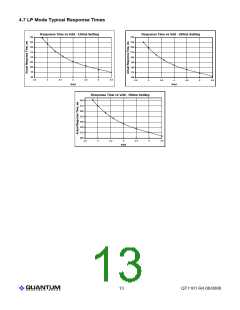
Response time - Fast mode
Response time - normal mode
Response time - LP mode
Release time - all modes
Serial communications speed
ms
40
ms
200
40
ms
200ms LP setting
End of touch
Tdr
bps
ms
8,000
38,400
baud
4.4 DC Specifications
Vdd = 5.0V, Ta = recommended, Cx = 5pF, Cs = 4.7nF, Ta = recommended range; circuit of Figure 1.1 unless noted
Parameter Description
Min
Typ
Max
Units
Notes
Iddn
Average supply current,
normal mode*
4.5
2.7
2.1
1.9
1.5
8
mA
@ Vdd = 5.0
@ Vdd = 4.0
@ Vdd = 3.6
@ Vdd = 3.3
@ Vdd = 2.8
Iddl
Average supply current,
LP mode*
75
µA
@ Vdd = 3.0; 200ms LP mode
Vdds
Average supply turn-on slope
100
V/s
Req’d for startup, w/o external reset
ckt
Vil
Vhl
Vol
Voh
Iil
Low input logic level
High input logic level
Low output voltage
High output voltage
Input leakage current
Acquisition resolution
0.7
0.5
±1
V
V
3.5
V
7mA sink
Vdd-0.5
V
2.5mA source
µA
bits
Ar
8
*No spread spectrum circuit
Lq
10
QT1101 R4.06/0806

 QUANTUM [ QUANTUM RESEARCH GROUP ]