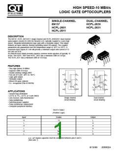
HIGH SPEED-10 MBit/s
LOGIC GATE OPTOCOUPLERS
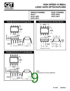
SINGLE-CHANNEL
6N137
DUAL-CHANNEL
HCPL-2630
HCPL-2601
HCPL-2611
HCPL-2631
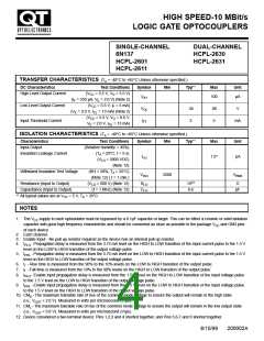
TRANSFER CHARACTERISTICS (TA = -40°C to +85°C Unless otherwise specified.)
DC Characteristics
Test Conditions
(VCC = 5.5 V, VO = 5.5 V)
Symbol
Min
Typ**
Max
Unit
High Level Output Current
IOH
100
µA
(IF = 250 µA, VE = 2.0 V) (Note 2)
(VCC = 5.5 V, IF = 5 mA)
Low Level Output Current
Input Threshold Current
VOL
IFT
.35
3
.06
5
V
(VE = 2.0 V, ICL = 13 mA) (Note 2)
(VCC = 5.5 V, VO = 0.6 V,
mA
VE = 2.0 V, IOL = 13 mA)
ISOLATION CHARACTERISTICS (TA = -40°C to +85°C Unless otherwise specified.)
Characteristics
Test Conditions
(Relative humidity = 45%)
(TA = 25°C, t = 5 s)
(VI-O = 3000 VDC)
Symbol
Min
Typ**
Max
Unit
Input-Output
Insulation Leakage Current
II-O
1.0*
µA
(Note 12)
Withstand Insulation Test Voltage
(RH < 50%, TA = 25°C)
(Note 12) ( t = 1 min.)
(VI-O = 500 V) (Note 12)
(f = 1 MHz) (Note 12)
VISO
2500
VRMS
Resistance (Input to Output)
Capacitance (Input to Output)
RI-O
CI-O
1012
0.6
!
pF
** All typical values are at VCC = 5 V, TA = 25°C
NOTES
1. The VCC supply to each optoisolator must be bypassed by a 0.1µF capacitor or larger. This can be either a ceramic or solid tantalum
capacitor with good high frequency characteristic and should be connected as close as possible to the package VCC and GND pins
of each device.
2. Each channel.
3. Enable Input - No pull up resistor required as the device has an internal pull up resistor.
4. tPLH - Propagation delay is measured from the 3.75 mA level on the HIGH to LOW transition of the input current pulse to the 1.5 V
level on the LOW to HIGH transition of the output voltage pulse.
5. tPHL - Propagation delay is measured from the 3.75 mA level on the LOW to HIGH transition of the input current pulse to the 1.5 V
level on the HIGH to LOW transition of the output voltage pulse.
6. tr - Rise time is measured from the 90% to the 10% levels on the LOW to HIGH transition of the output pulse.
7. tf - Fall time is measured from the 10% to the 90% levels on the HIGH to LOW transition of the output pulse.
8. tELH - Enable input propagation delay is measured from the 1.5 V level on the HIGH to LOW transition of the input voltage pulse
to the 1.5 V level on the LOW to HIGH transition of the output voltage pulse.
9. tEHL - Enable input propagation delay is measured from the 1.5 V level on the LOW to HIGH transition of the input voltage pulse
to the 1.5 V level on the HIGH to LOW transition of the output voltage pulse.
10. CMH - The maximum tolerable rate of rise of the common mode voltage to ensure the output will remain in the high state
(i.e., VOUT > 2.0 V). Measured in volts per microsecond (V/µs).
11. CML - The maximum tolerable rate of rise of the common mode voltage to ensure the output will remain in the low output state
(i.e., VOUT < 0.8 V). Measured in volts per microsecond (V/µs).
12. Device considered a two-terminal device: Pins 1,2,3 and 4 shorted together, and Pins 5,6,7 and 8 shorted together.
8/10/99
200002A

 QT [ QT OPTOELECTRONICS ]