PDF
最近搜索
热门搜索
发布采购

| 型号: | ASM3P622S00JG-08-TT |
| PDF下载: | 下载PDF文件 查看货源 |
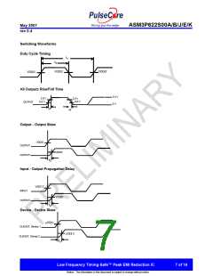
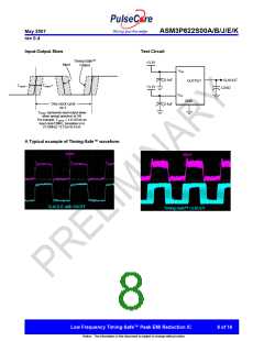
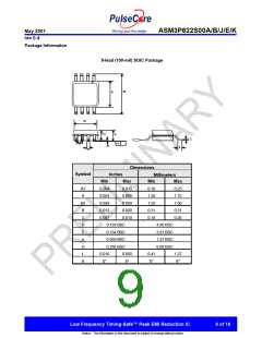
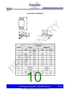
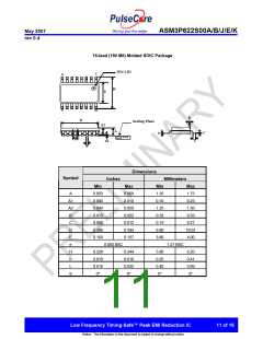
| 内容描述: | 低频定时- SAFE™峰值EMI降低IC [Low Frequency Timing-Safe™ Peak EMI reduction IC] |
| 分类和应用: | |
| 文件页数/大小: | 16 页 / 712 K |
| 品牌: |  PULSECORE [ PulseCore Semiconductor ] PULSECORE [ PulseCore Semiconductor ] |
专业IC领域供求交易平台:提供全面的IC Datasheet资料和资讯,Datasheet 1000万数据,IC品牌1000多家。