PE42420
Product Specification
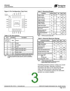
Figure 3. Pin Configuration (Top View)
Table 3. Operating Ranges
Parameter
Supply voltage
Symbol Min
Typ
Max Unit
VDD
IDD
2.7
5.5
V
Supply current
VDD = 2.7 to 5.5V
120
200
µA
Digital input high
(CTRL1, CTRL2)
VIH
1.17
-0.3
3.6
V
Digital input low
(CTRL1, CTRL2)
VIL
ICTRL
PIN
0.6
12
30
V
Digital input current
9
µA
Maximum operating power
(RFC-RFX)1
dBm
Maximum power into
termination (RFX)1
PMAX
TOP
20
dBm
°C
Operating temperature
range
-40
+85
Table 2. Pin Descriptions
Notes: 1. 100% duty cycle, all bands, 50Ω
Pin #
Pin Name
Description
Table 4. Absolute Maximum Ratings
1, 2, 4-7, 9,
10-12, 14,
15, 18, 19
GND
Ground
Parameter/Condition
Supply voltage
Symbol Min Max
Unit
VDD
-0.3
-0.3
5.5
V
3
8
RF11
RFC1
RF21
RF port
Digital input voltage
(CTRL1, CTRL2)
VCTRL
3.6
V
RF common
RF port
13
16
17
20
Pad
Operating power
(RFC-RFX)1
PIN
30
20
dBm
CTRL2 Digital control logic input 2
CTRL1 Digital control logic input 1
Power into termination (RFX)1
PMAX
TST
dBm
°C
Storage temperature range
-65 +150
+125
VDD
Supply voltage
Maximum die junction temperature
TJmax
°C
GND
Exposed pad: ground for proper operation
ESD voltage HBM2
RFC
Note 1: RF pins 3, 8 and 13 must be at 0V DC. The RF pins do not require
DC blocking capacitors for proper operation if the 0V DC requirement
is met
VESD
VESD
4000
2000
V
V
All other pins
ESD voltage MM3, all pins
100
V
Notes: 1. 100% duty cycle, all bands, 50Ω
2. Human Body Model (MIL-STD 883 Method 3015)
3. Machine Model (JEDEC JESD22-A115)
Exceeding absolute maximum ratings may cause
permanent damage. Operation should be
restricted to the limits in the Operating Ranges
table. Operation between operating range
maximum and absolute maximum for extended
periods may reduce reliability.
Document No. DOC-14514-2 │ www.psemi.com
©2010-2013 Peregrine Semiconductor Corp. All rights reserved.
Page 3 of 11

 PSEMI [ Peregrine Semiconductor ]