TOP252-262
Auto-Restart
+
78
For RIL = 12 k7
ILIMIT = 61%
Slope = PWM Gain
(constant over load range)
For RIL = 19 k7
ILIMIT = 37%
DC
Input
Voltage
See Figure 55b for other
resistor values (RIL) to
select different ILIMIT values.
D
S
M
CONTROL
C
RIL
CONTROL
Current
-
PI-4713-021308
100
55
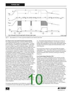
Figure 8. P/G Package Externally Set Current Limit.
reduction, output overvoltage protection (OVP), external current
limit adjustment, remote ON/OFF and device reset. A
connection to SOURCE pin disables all functions on this pin
and makes TOPSwitch-HX operate in simple three terminal
mode (like TOPSwitch-II).
25
CONTROL
Current
FREQUENCY (F) Pin (TOP254-258Y, and all E and L packages):
Input pin for selecting switching frequency 132 kHz if connected
to SOURCE pin and 66 kHz if connected to CONTROL pin.
The switching frequency is internally set for fixed 66 kHz
operation in the P, G, M package and TOP259YN, TOP260YN
and TOP261YN.
Full Frequency Mode
132
66
Low
Frequency
Mode
Variable
Frequency
Mode
SIGNAL GROUND (G) Pin (TOP259YN, TOP260YN &
TOP261YN only):
Return for C pin capacitor and X pin resistor.
Multi-Cycle
Modulation
Jitter
30
SOURCE (S) Pin:
Output MOSFET source connection for high voltage power
return. Primary side control circuit common and reference point.
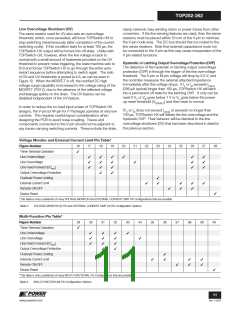
CONTROL
IC03 ICOFF
ICD1 IB
IC01
IC02
Current
PI-4645-041107
Figure 9. Control Pin Characteristics (Multi-Mode Operation).
TOPSwitch-HX Family Functional Description
Like TOPSwitch-GX, TOPSwitch-HX is an integrated switched
mode power supply chip that converts a current at the control
input to a duty cycle at the open drain output of a high voltage
power MOSFET. During normal operation the duty cycle of the
power MOSFET decreases linearly with increasing CONTROL
pin current as shown in Figure 9.
two terminals, VOLTAGE-MONITOR and EXTERNAL CURRENT
LIMIT (available in M package) or one terminal MULTI-FUNCTION
(available in P and G package) have been used to implement
some of the new functions. These terminals can be connected
to the SOURCE pin to operate the TOPSwitch-HX in a
TOPSwitch-like three terminal mode. However, even in this three
terminal mode, the TOPSwitch-HX offers many transparent
features that do not require any external components:
In addition to the three terminal TOPSwitch features, such as
the high voltage start-up, the cycle-by-cycle current limiting,
loop compensation circuitry, auto-restart and thermal
shutdown, the TOPSwitch-HX incorporates many additional
functions that reduce system cost, increase power supply
performance and design flexibility. A patented high voltage
CMOS technology allows both the high-voltage power MOSFET
and all the low voltage control circuitry to be cost effectively
integrated onto a single monolithic chip.
1. A fully integrated 17 ms soft-start significantly reduces or
eliminates output overshoot in most applications by sweeping
both current limit and frequency from low to high to limit the
peak currents and voltages during start-up.
2. A maximum duty cycle (DCMAX) of 78% allows smaller input
storage capacitor, lower input voltage requirement and/or
higher power capability.
3. Multi-mode operation optimizes and improves the power
supply efficiency over the entire load range while maintaining
good cross regulation in multi-output supplies.
Three terminals, FREQUENCY, VOLTAGE-MONITOR, and
EXTERNAL CURRENT LIMIT (available in Y and E/L packages),
7
www.powerint.com
Rev. F 01/09

 POWERINT [ Power Integrations ]