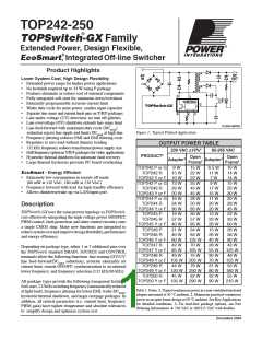
TOP242-250
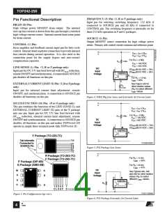
FREQUENCY (F) Pin: (Y, R or F package only)
Pin Functional Description
Input pin for selecting switching frequency: 132 kHz if
connected to SOURCE pin and 66 kHz if connected to
CONTROL pin. The switching frequency is internally set for
fixed 132 kHz operation in P and G packages.
DRAIN (D) Pin:
High voltage power MOSFET drain output. The internal
start-up bias current is drawn from this pin through a switched
high-voltage current source. Internal current limit sense point
for drain current.
SOURCE (S) Pin:
Output MOSFET source connection for high voltage power
return. Primary side control circuit common and reference point.
CONTROL (C) Pin:
Error amplifier and feedback current input pin for duty cycle
control. Internal shunt regulator connection to provide internal
bias current during normal operation. It is also used as the
connection point for the supply bypass and auto-restart/
compensation capacitor.
VUV = IUV x RLS
VOV = IOV x RLS
+
For RLS = 2 MΩ
2 MΩ
RLS
VUV = 100 VDC
VOV = 450 VDC
LINE-SENSE (L) Pin: (Y, R or F package only)
Input pin for OV, UV, line feed forward with DCMAX reduction,
remoteON/OFFandsynchronization. AconnectiontoSOURCE
pin disables all functions on this pin.
DC
Input
Voltage
DCMAX@100 VDC = 78%
DCMAX@375 VDC = 38%
D
S
L
CONTROL
C
For RIL = 12 kΩ
ILIMIT = 69%
X
EXTERNALCURRENTLIMIT(X)Pin:(Y,RorFpackage
only)
Input pin for external current limit adjustment, remote
ON/OFF, and synchronization. A connection to SOURCE pin
disables all functions on this pin.
See Figure 54b for
other resistor values
(RIL) to select different
ILIMIT values
RIL
12 kΩ
-
Figure 4. Y/R/F Pkg Line Sense and Externally Set Current Limit.
MULTI-FUNCTION (M) Pin: (P or G package only)
This pin combines the functions of the LINE-SENSE (L) and
EXTERNAL CURRENT LIMIT (X) pins of the Y package
into one pin. Input pin for OV, UV, line feed forward with
DCMAX reduction, external current limit adjustment, remote
ON/OFF and synchronization. A connection to SOURCE pin
disables all functions on this pin and makes TOPSwitch-GX
operate in simple three terminal mode (like TOPSwitch-II).
+
VUV = IUV x RLS
VOV = IOV x RLS
For RLS = 2 MΩ
VUV = 100 VDC
VOV = 450 VDC
RLS
2 MΩ
DC
Input
Voltage
DCMAX@100 VDC = 78%
DCMAX@375 VDC = 38%
D
S
M
CONTROL
C
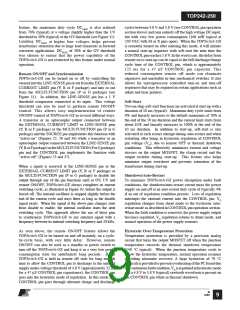
Y Package (TO-220-7C)
-
Tab Internally
Connected to
SOURCE Pin
7 D
PI-2509-040501
5 F
4 S
3 X
2 L
1 C
Figure 5. P/G Package Line Sense.
+
R Package (TO-263-7C)
F Package (TO-262-7C)
For RIL = 12 kΩ
ILIMIT = 69%
P Package (DIP-8B)
G Package (SMD-8B)
For RIL = 25 kΩ
ILIMIT = 43%
DC
Input
Voltage
M
S
S
S
1
2
8
7
See Figures 54b, 55b
and 56b for other resistor
values (RIL) to select
different ILIMIT values.
D
S
M
S
C
3
4
CONTROL
C
RIL
5
D
1 2 3 4 5
7
C L X S F D PI-2724-010802
-
PI-2517-022604
Figure 3. Pin Configuration (top view).
Figure 6. P/G Package Externally Set Current Limit.
M
4
12/04

 POWERINT [ Power Integrations ]