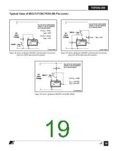
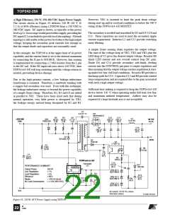
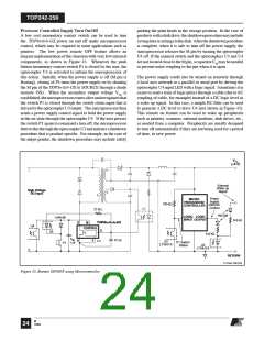
TOP242-250
to the relatively large size of C2). An optional MOV (RV1)
extends the differential surge protection to 6 kV from 4 kV.
Multiple Output, 60 W, 185-265 VAC Input Power Supply
Figure 44 shows a multiple output supply typical for high end
set-top boxes or cable decoders containing high capacity hard
disks for recording. The supply delivers an output power of
45 W continuous/60 W peak (thermally limited) from an input
voltage of 185 VAC to 265 VAC. Efficiency at 45 W,
185 VAC is ≥ 75%.
Leakage inductance clamping is provided by VR1, R5 and C5,
keeping the DRAIN voltage below 700 V under all conditions.
Resistor R5 and capacitor C5 are selected such that VR1
dissipates very little power except during overload conditions.
The frequency jittering feature of TOPSwitch-GX allows the
circuit shown to meet CISPR22B with simple EMI filtering
(C1, L1 and C6) and the output grounded.
The 3.3 V and 5 V outputs are regulated to ±5% without
the need for secondary linear regulators. DC stacking (the
secondary winding reference for the other output voltages is
connected to the cathode of D10 rather than the anode) is used
to minimize the voltage error for the higher voltage outputs.
The secondaries are rectified and smoothed by D7 to D11, C7,
C9, C11, C13, C14, C16 and C17. Diode D11 for the 3.3 V
output is a Schottky diode to maximize efficiency. Diode D10
for the 5 V output is a PN type to center the 5 V output at 5 V.
The 3.3 V and 5 V output require two capacitors in parallel to
meet the ripple current requirement. Switching noise filtering
is provided by L2 to L5 and C8, C10, C12, C15 and C18.
Resistor R6 prevents peak charging of the lightly loaded 30 V
output. The outputs are regulated using a secondary reference
(U3). Both the 3.3 V and 5 V outputs are sensed via R11
and R10. Resistor R8 provides bias for U3 and R7 sets the
overall DC gain. Resistor R9, C19, R3 and C5 provide loop
compensation. A soft-finish capacitor (C20) eliminates output
overshoot.
Due to the high ambient operating temperature requirement
typical of a set-top box (60 °C), the TOP246Y is used to
reduce conduction losses and minimize heatsink size. Resistor
R2 sets the device current limit to 80% of typical to limit
overload power. The line sense resistor (R1) protects the
TOPSwitch-GXfromlinesurgesandtransientsbysensingwhen
the DC rail voltage rises to above 450 V. In this condition the
TOPSwitch-GX stops switching, extending the input voltage
withstand to 496 VAC, which is ideal for countries with
poor power quality. A thermistor (RT1) is used to prevent
premature failure of the fuse by limiting the inrush current (due
R6
10 Ω
D7
UF4003
PERFORMANCE SUMMARY
30 V @
0.03 A
Output Power:
Regulation:
3.3 V:
5 V:
12 V:
45 W Cont./60 W Peak
C7
C8
L2
3.3 µH
3A
47 µF
10 µF
50 V
D8
50 V
UF5402
± 5%
± 5%
± 7%
± 7%
± 8%
≥75%
0.6 W
18 V @
0.5 A
C9
C10
L3
3.3 µH
3A
330 µF
100 µF
D9
UF5402
25 V
18 V:
30 V:
25 V
12 V @
0.6 A
C11
C16
1000 µF
25 V
C13
1000 µF
25 V
C12
100 µF
25 V
Efficiency:
No Load Consumption:
C6
2.2 nF
Y1
390 µF
L4
3.3 µH
5A
35 V
5 V @
3.2 A
VR1
P6KE170
R5
68 kΩ
2 W
C14
C15
220 µF
16 V
L5
3.3 µH
5A
1000 µF
D10
BYV32-200
25 V
3.3 V @
3 A
C5
1 nF
400 V
C18
D11
MBR1045
C17
1000 µF
25 V
220 µF
16 V
D1-D4
1N4007 V
RTN
D6
1N4937
C2
L1
20 mH
0.8A
68 µF
400 V
R10
D6
1N4148
C3
1 µF
50 V
R7
150 Ω
15.0
R1
kΩ
2 MΩ
C1
0.1 µF
X1
U2
LTV817
T1
1/2 W
R8
1 kΩ
R11
9.53
kΩ
TOPSwitch-GX
D
S
L
RV1
275 V
14 mm
TOP246Y
U1
CONTROL
CONTROL
C19
0.1 µF
R9
3.3 kΩ
C
F1
3.15 A
C3
0.1 µF
50 V
R3
6.8 Ω
X
F
J1
RT1
C20
22 µF
10 V
10 Ω
U3
TL431
C5
47 µF
10 V
R2
9.08 kΩ
L
1.7 A
R12
10 k
PI-2693-081704
N
Figure 44. 60 W Multiple Output Power Supply using TOP246.
M
12/04
23

 POWERINT [ Power Integrations ]