TOP221-227
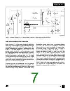
L1
3.3 µH
D2
UF5401
+5 V
RTN
C2
C3
+
330 µF
100 µF
R3
47 kΩ
C1
2.2 nF
1 kV
VR1
10 V
10 V
D1
UF4005
R2
100 Ω
D3
1N4148
R1
10 Ω
Wide-Range
DC Input
T1
+
U1
C4
100 µF
16 V
D
TOP221P
TOPSwitch-II
C
CONTROL
U2
PC817A
12 V Non-Isolated
C5
S
47 µF
10 V
-
-
PI-2115-040401
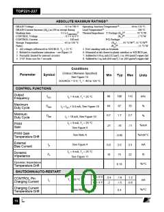
Figure 7. Schematic Diagram of a 4 W TOPSwitch-II Standby Power Supply using an 8 lead PDIP.
Application Examples
Following are just two of the many possible TOPSwitch
implementations. Refer to the Data Book and Design Guide
for additional examples.
vary from 100 V to 380 V DC which corresponds to the full
universal AC input range. The TOP221 is packaged in an 8 pin
power DIP package.
4 W Standby Supply using 8 Lead PDIP
The output voltage (5 V) is directly sensed by the Zener diode
(VR1)andtheoptocoupler(U2). Theoutputvoltageisdetermined
by the sum of the Zener voltage and the voltage drop across the
LEDoftheoptocoupler(thevoltagedropacrossR1isnegligible).
The output transistor of the optocoupler drives the CONTROL
pinoftheTOP221. C5bypassestheCONTROLpinandprovides
control loop compensation and sets the auto-restart frequency.
Figure 7 shows a 4 W standby supply. This supply is used in
appliances where certain standby functions (e.g. real time
clock, remote control port) must be kept active even while the
main power supply is turned off.
The 5 V secondary is used to supply the standby function and
the 12 V non-isolated output is used to supply power for the
PWM controller of the main power supply and other primary
side functions.
Thetransformer’sleakageinductancevoltagespikesaresnubbed
by R3 and C1 through diode D1. The bias winding is rectified
and filtered by D3 and C4 providing a non-isolated 12 V output
which is also used to bias the collector of the optocoupler’s
output transistor. The isolated 5 V output winding is rectified by
D2 and filtered by C2, L1 and C3.
For this application the input rectifiers and input filter are sized
for the main supply and are not shown. The input DC rail may
D
7/01
6

 POWERINT [ Power Integrations ]