TNY375-380
Absolute Maximum Ratings(1,4)
DRAIN Voltage ....................................................-0.3 V to 700 V Lead Temperature(3) ........................................................260 °C
DRAIN Peak Current: TNY37ꢀ...................................... 0.6 A(ꢀ)
TNY376...................................... 0.8 A(ꢀ) Notes:
TNY377...................................... 1.4 A(ꢀ) 1. All voltages referenced to SOURCE, TA = 2ꢀ °C.
TNY378.......................................2.2 Aꢀ) 2. Normally limited by internal circuitry.
TNY379...................................... 2.9 A(ꢀ) 3. 1/16 in. from case for ꢀ seconds.
TNY380...................................... 4.3 A(ꢀ) 4. Maximum ratings specified may be applied one at a time
EN/UV Voltage ....................................................... -0.3 V to 9 V
EN/UV Current .............................................................. 100 mA
BP/M Voltage .................................................. ......-0.3 V to 9 V
without causing permanent damage to the product.
Exposure to Absolute Maximum Rating conditions for
extended periods of time may affect product reliability.
Storage Temperature ...................................... -6ꢀ °C to 1ꢀ0 °C ꢀ. The peak DRAIN current is allowed while the DRAIN voltage is
Operating Junction Temperature(2)................... -40 °C to 1ꢀ0 °C
simultaneously less than 400 V.
Thermal Impedance
Thermal Impedance: P or G Package:
Notes:
(qJA) ................................70 °C/W(2); 60 °C/W(3) 1. Measured on the SOURCE pin close to plastic interface.
(qJC)(1) ............................................... ..11 °C/W 2. Soldered to 0.36 sq. in. (232 mm2), 2 oz. (610 g/m2) copper
D Package:
clad.
(qJA) ..............................100 °C/W(2); 80 °C/W(3) 3. Soldered to 1 sq. in. (64ꢀ mm2), 2 oz. (610 g/m2) copper
(qJC)(2) ............................ .....................30 °C/W clad.
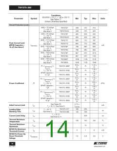
Conditions
SOURCE = 0 V; TJ = -40 to 12ꢀ °C
Parameter
Symbol
Min
Typ
Max
Units
See Figure 17
(Unless Otherwise Specified)
Control Functions
State Machine at
Highest Current
Limit Level
Average
248
264
280
fOSC
pk-pk Jitter
16
Output Frequency
See Note A
TJ = 2ꢀ °C
kHz
All Lower Current
Limit Levels
Average
132
fOSC-Low
DCMAX
pk-pk Jitter
8
TJ = 2ꢀ °C
Maximum Duty Cycle
S1 Open
62
6ꢀ
5
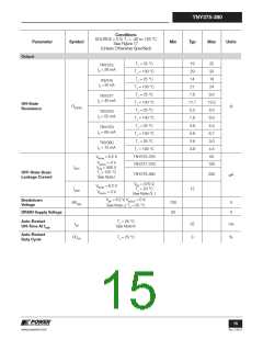
EN/UV Pin Upper
Turnoff Threshold
Current
IDIS
-1ꢀ0
-11ꢀ
-90
mA
IEN/UV = 2ꢀ mA
IEN/UV = -2ꢀ mA
1.8
0.8
2.2
1.2
2.6
1.6
EN/UV Pin Voltage
VEN
V
EN/UV Current > IDIS (MOSFET Not
Switching) See Note B
IS1
290
mA
TNY37ꢀ
38ꢀ
460
ꢀ70
740
870
1100
ꢀ20
600
TNY376
EN/UV Open
DRAIN Supply Current
TNY377
710
(MOSFET
Switching at fOSC
IS2
mA
)
TNY378
TNY379
TNY380
900
See Note C
1060
13ꢀ0
12
Rev. C 09/12
www.powerint.com

 POWERINT [ Power Integrations ]