LNK362-364
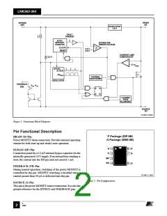
DRAIN
(D)
BYPASS
(BP)
REGULATOR
5.8 V
FAULT
PRESENT
AUTO-
RESTART
COUNTER
BYPASS PIN
UNDER-VOLTAGE
+
-
CLOCK
RESET
5.8 V
4.8 V
CURRENT LIMIT
COMPARATOR
6.3 V
+
-
V
ILIMIT
JITTER
CLOCK
DCMAX
THERMAL
SHUTDOWN
OSCILLATOR
FEEDBACK
VFB -VTH
(FB)
S
R
Q
Q
LEADING
EDGE
BLANKING
SOURCE
(S)
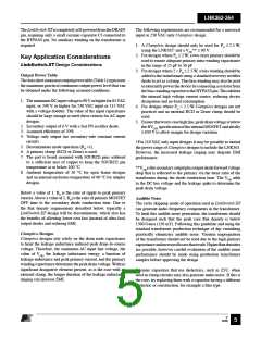
PI-4232-110205
Figure 2. Functional Block Diagram.
Pin Functional Description
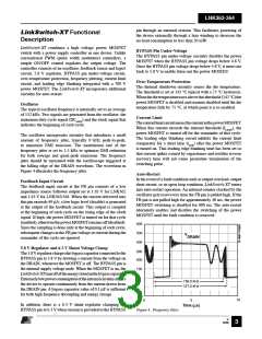
P Package (DIP-8B)
G Package (SMD-8B)
DRAIN (D) Pin:
Power MOSFET drain connection. Provides internal operating
current for both start-up and steady-state operation.
S
S
S
S
1
2
8
7
BYPASS (BP) Pin:
Connection point for a 0.1 µF external bypass capacitor for the
internally generated 5.8 V supply. If an external bias winding is
used, the current into the BP pin must not exceed 1 mA.
BP
FB
3
4
5
D
FEEDBACK (FB) Pin:
During normal operation, switching of the power MOSFET is
controlled by this pin. MOSFET switching is disabled when a
current greater than 49 µA is delivered into this pin.
PI-3491-111903
Figure 3. Pin Configuration.
SOURCE (S) Pin:
This pin is the power MOSFET source connection. It is also the
ground reference for the BYPASS and FEEDBACK pins.
C
12/05
2

 POWERINT [ Power Integrations ]