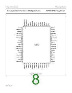
Philips Semiconductors
Product specification
New In Car Entertainment (NICE) car radio
TEA6845AH; TEA6845H
7.3.5
AM NOISE DETECTOR AND BLANKER
If the test mode is enabled by pin fref:
• The settling time of the AM IF2 AGC is reduced to less
than 100 ms in the nominal application
The detection point for the AM noise blanker is the output
stage of AM mixer 1, while blanking is realized at the
output of the mixer 2.
• The digital-to-analog converters for the antenna DAA
and the level DAA can be clocked directly by the SCL
line of the I2C-bus
• The output at pin fref can be selected by the I2C-bus:
TEA6880H or TEF6890H reference frequency, PLL
reference frequency or PLL programmable divider
output frequency
Trigger sensitivity can be modified by changing the resistor
value at pin AMNBHOLD.
7.3.6
FM AND AM LEVEL DETECTOR
FM and AM level detectors provide the temperature
compensated output voltage. The starting points and
slopes of the level detector outputs are programmable via
the I2C-bus.
• The RDS update control circuit can be clocked directly
via pin DAATD
• Pin T1AMAGC can be used to enable the load PLL
7.4
Test mode
circuit of the RDS update control circuit
• Charge pumps can be set into 3-state mode.
The test mode of the IC is activated by:
• Sending the test byte (byte 5) to the IC
• Connecting pin fref through a 100 kΩ resistor to VDDA1
• Applying 50 µA to pin fref.
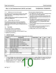
8
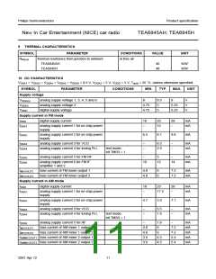
LIMITING VALUES
In accordance with the Absolute Maximum Rating System (IEC 60134).
SYMBOL
VDDA1
VDDA2
VDDA3
VDDA4
VDDA5
VDDA6
VDDD
PARAMETER
CONDITIONS
MIN.
−0.3
MAX.
+10
UNIT
analog supply voltage 1 for on-chip power supply
analog supply voltage 2 for on-chip power supply
analog supply voltage 3 for VCO
V
V
V
V
V
V
V
V
−0.3
−0.3
−0.3
−0.3
−0.3
−0.3
−0.3
+6.5
+10
+10
+10
+10
+6.5
−
analog supply voltage 4 for tuning PLL
analog supply voltage 5 for FM and AM RF
analog supply voltage 6 for IF amplifier 1 and 2
digital supply voltage
∆VDD8.5-DD5 difference between any 8.5 V supply voltage and any note 1
5 V supply voltage
Tstg
Tamb
Ves
storage temperature
−55
+150
+85
°C
°C
V
ambient temperature
−40
electrostatic handling voltage
note 2
note 3
−200
−2000
+200
+2000
V
Notes
1. To avoid damages and wrong operation it is necessary to keep all 8.5 V supply voltages at a higher level than any
5 V supply voltage. This is also necessary during power-on and power-down sequences. Precautions have to be
provided in such a way that interferences can not pull down the 8.5 V supply below the 5 V supply.
2. Machine model (R = 0 Ω, C = 200 pF).
3. Human body model (R = 1.5 kΩ, C = 100 pF).
2001 Apr 12
10

 NXP [ NXP ]