This text is here in white to force landscape pages to be rotated correctly when browsing through the pdf in the Acrobat reader.This text is here in
_white to force landscape pages to be rotated correctly when browsing through the pdf in the Acrobat reader.This text is here inThis text is here in
white to force landscape pages to be rotated correctly when browsing through the pdf in the Acrobat reader. white to force landscape pages to be ...
V
mode select
220 nF
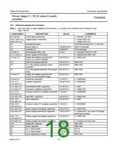
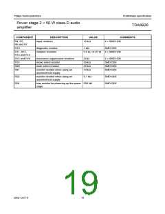
C1
C2
DDA
V
V
SSD
DDD
V
V
SSA
DDA
220 nF
V
R19
39 kΩ
R20
C10
560 pF
C11
560 pF
V
V
V
DD1 DD2
10
SS2 SS1
1
QGND
C18
39 kΩ
3
12
R11
5.6 Ω
R12
5.6 Ω
on
PWM2
SW2
MODE
17
13
14
16
D1
(5.6 V)
mute
off
6
1 nF
L2
−
OUT2
SW2
REL2
EN2
C44
220 nF
S1
17
16
14
11
12
1
Sumida 33 µH
CDRH127-330
REL2
EN2
OUT2
C8
15 nF
4 or 8 Ω
SE
R1
2
OSC
GND
7
R15
24 Ω
U2
V
U1
+
−
DDD
OUT2
BOOT2
C19
1 nF
27 kΩ
C14
V
SSA
C3
470 nF
R24
200 kΩ
V
DD1
V
5
C15
220 nF
STAB
DDD
TDA8929T
TDA8926J
or
TDA8927J
QGND
19
POWERUP
220 nF
V
DD2
15
9
OUT2
2
13
C4
220 nF
SGND1
SGND2
D2
(7.5 V)
2
C5
C7
220 nF
V
SS2
C6
220 nF
V
8 Ω
BTL
STAB
SSD
GND
GND
18
22
V
V
SSA
SSD
R10
1
11
C43
180 pF
220 nF
DIAG
10
8
+
OUT1
3
C17
220 nF
V
QGND
+
SS1
IN1
DIAGCUR
1 kΩ
V
5
CONTROLLER
POWER STAGE
SSD
C16
C22
C20
1 nF
470 nF
330 pF
R16
24 Ω
−
+
IN1
BOOT1
OUT1
−
OUT1
2
EN1
EN1
REL1
SW1
4
8
6
7
21
23
24
20
4
2
1
C9
15 nF
REL1
SW1
Sumida 33 µH
CDRH127-330
IN2
4 or 8 Ω
SE
1
C23
J5
J6
330 pF
L4
+
OUT1
−
IN2
PWM1
C21
1 nF
9
R13
R14
5.6 Ω
5.6 Ω
15
QGND
outputs
C25
470 nF
C24
470 nF
C26
470 nF
C27
470 nF
C12
560 pF
C13
560 pF
n.c.
V
V
SSD
DDD
R5
10 kΩ
R4
10 kΩ
R6
10 kΩ
R7
10 kΩ
L7
bead
QGND
V
C28
C29
L5
bead
DDA
C30
1 nF
V
C40
47 µF
(35 V)
1 nF
1 nF
DDD
C36
220 nF
C37
220 nF
C34
1500 µF
(35 V)
V
V
+
25 V
DD
C32
220 nF
R21
10 kΩ
1
2
3
GND
GND
input 1
input 2
C35
1500 µF
(35 V)
J1
J3
J2
J4
R22
9.1 kΩ
C33
220 nF
C41
47 µF
(35 V)
C38
220 nF
C39
220 nF
−
25 V
SS
QGND
QGND
V
SSD
bead
L6
C31
1 nF
V
inputs
SSA
V
SS
MLD633
power supply
QGND
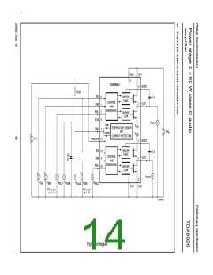
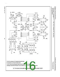
R21 and R22 are necessary only in BTL applications with asymmetrical supply.
BTL: remove R6, R7, C23, C26 and C27 and close J5 and J6.
C22 and C23 influence the low-pass frequency response and should be tuned with the real load (loudspeaker).
ahdnbok,uflapegwidt
Inputs floating or inputs referenced to QGND (close J1 and J4) or referenced to VSS (close J2 and J3) for an input signal ground reference.
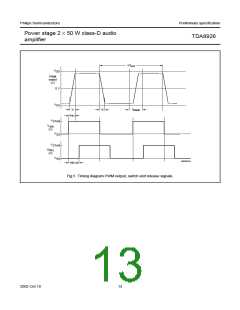
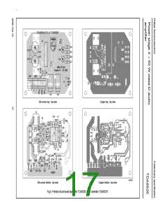
Fig.7 Two-chip class-D audio amplifier application diagram for TDA8926J and controller TDA8929T.

 NXP [ NXP ]