Philips Semiconductors
Preliminary specification
Power stage 2 × 50 W class-D audio
amplifier
TDA8926
14 SWITCHING CHARACTERISTICS
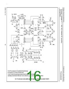
VP = ±25 V; Tamb = 25 °C; measured in Fig.6; unless otherwise specified.
SYMBOL
PARAMETER
CONDITIONS
MIN.
TYP. MAX. UNIT
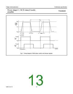
PWM outputs (pins OUT1 and OUT2); see Fig.5
tr
rise time
−
30
30
70
20
−
−
−
−
ns
ns
ns
ns
tf
fall time
−
−
−
tblank
tPD
blanking time
propagation delay
from pin SW1 (SW2) to
pin OUT1 (OUT2)
tW(min)
Rds(on)
minimum pulse width
note 1
−
−
220
0.2
270
0.3
ns
on-resistance of the output
transistors
Ω
Note
1. When used in combination with controller TDA8929T, the effective minimum pulse width during clipping is 0.5tW(min)
.
14.1 Duty factor
For the practical useable minimum and maximum duty factor (δ) which determines the maximum output power:
t
× fosc
t
W(min) × fosc
--W-----(--m---i-n---)---------------
2
× 100% < δ < 1 –
× 100%
-------------------------------
2
Using the typical values: 3.5% < δ < 96.5%.
2002 Oct 10
12

 NXP [ NXP ]