Philips Semiconductors
Preliminary specification
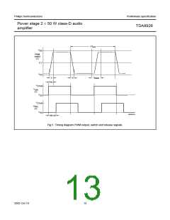
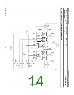
Power stage 2 × 50 W class-D audio
amplifier
TDA8926
12 DC CHARACTERISTICS
VP = ±25 V; Tamb = 25 °C; measured in test diagram of Fig.6; unless otherwise specified.
SYMBOL
Supply
PARAMETER
CONDITIONS
MIN.
TYP.
MAX.
UNIT
VP
supply voltage
total quiescent current
note 1
±15
±25
±30
V
Iq(tot)
no load connected
outputs floating
−
−
35
5
45
10
mA
mA
Internal stabilizer logic supply (pin STAB)
VO(STAB) stabilizer output voltage
Switch inputs (pins SW1 and SW2)
11
13
15
V
VIH
VIL
HIGH-level input voltage
LOW-level input voltage
referenced to VSS
referenced to VSS
10
0
−
−
VSTAB
2
V
V
Control outputs (pins REL1 and REL2)
VOH
VOL
HIGH-level output voltage
LOW-level output voltage
referenced to VSS
referenced to VSS
10
0
−
−
VSTAB
2
V
V
Diagnostic output (pin DIAG, open-drain)
VOL
ILO
LOW-level output voltage
output leakage current
IDIAG = 1 mA; note 2
no error condition
0
−
−
1.0
50
V
−
µA
Enable inputs (pins EN1 and EN2)
VIH
HIGH-level input voltage
LOW-level input voltage
hysteresis voltage
input current
referenced to VSS
referenced to VSS
−
0
−
−
9
5
4
−
VSTAB
−
V
VIL
V
VEN(hys)
II(EN)
−
V
300
µA
Switching-on input (pin POWERUP)
VPOWERUP
II(POWERUP)
operating voltage
input current
referenced to VSS
VPOWERUP = 12 V
5
−
12
V
−
100
170
µA
Temperature protection
Tdiag
Thys
temperature activating diagnostic VDIAG = VDIAG(LOW)
150
−
−
−
°C
°C
hysteresis on temperature
diagnostic
VDIAG = VDIAG(LOW)
−
20
Notes
1. The circuit is DC adjusted at VP = ±15 to ±30 V.
2. Temperature sensor or maximum current sensor activated.
2002 Oct 10
10

 NXP [ NXP ]