Philips Semiconductors
Product specification
Hi-fi stereo audio processor; I2C-bus
TDA8425
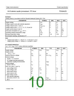
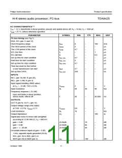
AC CHARACTERISTICS (1)
VCC = 12 V; bass/treble in linear position; pseudo and spatial stereo off; RL > 10 kΩ; CL < 1000 pF;
Tamb = 25 °C; unless otherwise specified
PARAMETER
I2C bus timing (see Fig.7)
SYMBOL
MIN.
TYP.
MAX.
UNIT
SDA, SCL (pin 11 and 12)
Clock frequency range
The HIGH period of the clock
The LOW period of the clock
SCL rise time
fSCL
0
4
−
−
−
−
−
−
−
−
100
kHz
tHIGH
tLOW
tr
−
µs
µs
µs
µs
µs
µs
µs
4.7
−
−
1
SCL fall time
tf
−
0.3
−
Set-up time for start condition
Hold time for start condition
Set-up time for stop condition
Time bus must be free before
a new transmission can start
Set-up time DATA
tSU; STA
tHD; STA
tSU; STO
4.7
4
−
4.7
−
tBUF
4.7
−
−
−
−
µs
tSU; DAT
250
ns
INPUTS
IN1 L (pin 18) IN1 R (pin 20);
IN2 L (pin 1) IN2 R (pin 3)
Input signal handling (RMS value)
at Vu = −12 dB; THD ≤ 0.5%
Input resistance
Vi(rms)
Ri
2
−
−
V
20
30
40
kΩ
Frequency response (−0,5 dB)
bass and treble in linear position;
stereo mode; effects off
f
20
−
20 000
Hz
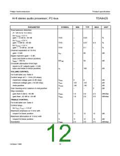
OUTPUTS
OUT R (pin 9); OUT L (pin 13)
Output voltage range (rms value)
at THD ≤ 0.7%; Vi(max) ≤ 2 V
Load resistance
Vo(rms)
RL
0.6
10
−
−
−
−
−
V
−
kΩ
Ω
Output impedance
ZO
100
Signal plus noise-to-noise ratio (weighted
according to CCIR 468-2); VO = 600 mV
gain = 6 dB
(S+N)/N
(S+N)/N
(S+N)/N
−
−
−
78
86
68
−
−
−
dB
dB
dB
gain = 0 dB
gain = ≤ −20 dB
Crosstalk between inputs at gain = 0 dB;
1 kHz; opposite inputs grounded (50 Ω);
IN1L (pin 18) to IN2L (pin1) or
IN1R (pin 20) to IN2R (pin 3)
αcr
−
100
−
dB
October 1988
11

 NXP [ NXP ]