Philips Semiconductors
Product specification
Triple video output amplifier
TDA6107Q
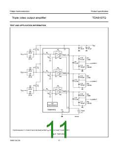
External flashover protection
Dissipation
For sufficient flashover protection it is necessary to apply
an external diode and 100 Ω resistor for each channel.
See application note “Application and Product description
of TDA6107Q/N1” (report number AN96072).
Regarding dissipation, distinction must first be made
between static dissipation (independent of frequency) and
dynamic dissipation (proportional to frequency).
The static dissipation of the TDA6107Q is due to voltage
supply currents and load currents in the feedback network
and CRT.
To limit the diode current an external 1 kΩ carbon
high-voltage resistor in series with the external diode and
a 2 kV spark gap are needed (for this resistor value, the
CRT has to be connected to the main PCB).
The static dissipation Pstat equals:
Pstat = VDD × IDD + 3 × VO(c) × IO(c)
VDD must be decoupled to GND:
Where:
1. With a capacitor >20 nF with good HF behaviour
(e.g. foil); this capacitor must be placed as close as
possible to pins 6 and 4, but definitely within 5 mm.
VDD = supply voltage
IDD = supply current
2. With a capacitor >3.3 µF on the picture tube base
VO(c) = DC value of cathode voltage
IO(c) = DC value of cathode current.
print.
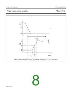
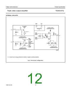
Switch-off behaviour
The dynamic dissipation Pdyn equals:
Pdyn = 3 × VDD × (CL + Cint) × fi × Vo(c)(p-p) × δ
The switch-off behaviour of the TDA6107Q is controllable.
This is due to the fact that the output pins of the
TDA6107Q are still under control of the input pins for low
power supply voltages (approximately 30 V and higher).
Where:
CL = load capacitance
Cint = internal load capacitance (≈4 pF)
fi = input frequency
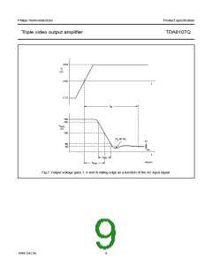
Bandwidth
The addition of the flash resistor produces a decreased
bandwidth and increases rise and fall times.
Vo(c)(p-p) = output voltage (peak-to-peak value)
δ = non-blanking duty cycle.
The IC must be mounted on the picture tube base print to
minimize the load capacitance CL.
1999 Oct 26
10

 NXP [ NXP ]